PCB Repair Logs Wonderboy: Difference between revisions
mNo edit summary |
mNo edit summary |
||
| (2 intermediate revisions by the same user not shown) | |||
| Line 4: | Line 4: | ||
<tr class="> | <tr class="> | ||
<td colspan="2" class="" style="text-align:center;">[[Image:marquee_wonderboy.jpg|200px]]</td> | <td colspan="2" class="" style="text-align:center;">[[Image:marquee_wonderboy.jpg|200px]]</td> | ||
</tr> | |||
<tr class=""> | |||
<th scope="row" style="text-align:left; white-space: nowrap;">Manufacturer</th> | |||
<td class="" style="">[[PCB_Manufacturers_Sega|Sega]]</td> | |||
</tr> | |||
<tr class=""> | |||
<th scope="row" style="text-align:left; white-space: nowrap;">Year</th> | |||
<td class="" style="">1986</td> | |||
</tr> | </tr> | ||
<tr class=""> | <tr class=""> | ||
| Line 11: | Line 19: | ||
<tr class=""> | <tr class=""> | ||
<th scope="row" style="text-align:left; white-space: nowrap;">Pin Out</th> | <th scope="row" style="text-align:left; white-space: nowrap;">Pin Out</th> | ||
<td class="" style=""> | <td class="" style="">[[PCB_Pinouts_Wonderboy|Wonderboy]]</td> | ||
</tr> | </tr> | ||
| Line 290: | Line 298: | ||
===Board 4=== | ===Board 4=== | ||
'''Repairer:''' [http://www.aussiearcade.com.au/member.php/1983-Womble Womble]<br> | |||
'''Forum Thread:''' [http://www.aussiearcade.com.au/showthread.php/14991-Wonderboy-Bootleg-Repair Wonderboy PCB Repair]<br> | |||
<br> | <br> | ||
Another Sega Wonderboy PCB saved from the scrap bin. | Another Sega Wonderboy PCB saved from the scrap bin. | ||
| Line 333: | Line 344: | ||
One more board left to fix - that one has everything ok except the enemy sprites are totally missing. Logic weirdy somewhere I would think. | One more board left to fix - that one has everything ok except the enemy sprites are totally missing. Logic weirdy somewhere I would think. | ||
<br> | <br> | ||
===Board 5=== | |||
'''Repairer:''' [http://www.aussiearcade.com.au/member.php/1983-Womble Womble]<br> | |||
'''Forum Thread:''' [http://www.aussiearcade.com.au/showthread.php/46682-Wonderboy-Repair-Log Wonderboy PCB Repair]<br> | |||
<br> | |||
Had Gt-rays Wonderboy in for some TLC recently. | |||
<br> | |||
<br> | |||
[[File:Pcb repair wonderboy 5 1.jpg]] | |||
<br> | |||
<br> | |||
The board was in good nick, a couple of chips had been replaced by Gt-ray himself in an attempt to fix the board. The chips replaced were ones I had found to be faulty in previous repairs. This approach is not likely to lead to success as there are many chips involved in any single thing you see on the screen, so even if the fault is similar the chances the exact same chip is the cause is pretty low. | |||
Aside from those chips there was this at IC55 and IC69... | |||
<br> | |||
<br> | |||
[[File:Pcb repair wonderboy 5 2.jpg]] | |||
<br> | |||
<br> | |||
...little links of burnt wire badly soldered across a couple of chips - very odd. | |||
As I had foolishly sold my Sega System 2 adaptor with my last Wonderboy board I had to make up another one to even power this up, a very tedious job, this one isn't going anywhere as I hate making up these things. It's such a dull job that I only wired up the power lines, the video and the sound at this stage, enough to power up the board and see what it does. | |||
<br> | |||
<br> | |||
[[File:Pcb repair wonderboy 5 3.jpg]] | |||
<br> | |||
<br> | |||
As expected, it was not well... | |||
<br> | |||
<br> | |||
{{#ev:youtube|L5zgzdLsalE}} | |||
<br> | |||
<br> | |||
[[File:Pcb repair wonderboy 5 4.jpg]] | |||
<br> | |||
<br> | |||
[[File:Pcb repair wonderboy 5 5.jpg]] | |||
<br> | |||
<br> | |||
[[File:Pcb repair wonderboy 5 6.jpg]] | |||
<br> | |||
<br> | |||
[[File:Pcb repair wonderboy 5 7.jpg]] | |||
<br> | |||
<br> | |||
[[File:Pcb repair wonderboy 5 8.jpg]] | |||
<br> | |||
<br> | |||
... aside from the messed up colours which seemed to change at random, the screen was very glitchy and covered with noise from time to time. | |||
First thing to do was to undo the crazyness on the LS85. | |||
<br> | |||
<br> | |||
[[File:Pcb repair wonderboy 5 9.jpg]] | |||
<br> | |||
<br> | |||
I had assumed that this was to connect up an unused gate on the chip to take over from a bad gate that the PCB connected to. Often TTL chips contain the same gate two, four or six times and in many cases the board doesn't use them all. However this wiring makes no sense whatsoever as the chip is a 74LS85, a single device and tying these lines together is going to bugger up the function of the chip entirely by joining four input lines to ground, (actually only 3 as one of the wires was just not actually soldered to anything on one end). | |||
After trying to see any sense in what had been done I simply removed the chip and the bits of wire, fully expecting to find the chip was bad. Except it wasn't, my VP280 EPROM reader gave the LS85 a clean bill of health, and despite it being a Fujitsu TTL chip it went back on the board. 74LS85s are not common chips on arcade boards and I couldn't find a single one in my scrap PCB bin. The game was such a mess and so unstable when running that I couldn't actually tell if this had made any difference at all. | |||
I had a poke around the video mixer section of the board with the scope and didn't find anything that looked bad, but as there were a collection of Fujitsu 74LS153 multiplexer chips in that area I fired up the HP 10529A logic comparator to compare a known good ls153 with the ones on the board. Due to the complexity of the 153 (12 input data streams producing 2 outputs data streams) it is impossible to see if it is doing the right thing with a scope, or a logic probe. As long as the output signal looks healthy you have no way to tell if the actual data it represents is bad, without feeding the same inputs to a known good chip and comparing the outputs to the on-board chip - which is exactly what this device does. | |||
<br> | |||
<br> | |||
[[File:Pcb repair wonderboy 5 10.jpg]] | |||
<br> | |||
<br> | |||
The LS153 at IC8 was bad, giving a constant mismatch between it and a good chip. So this was de-soldered and a good one soldered in its place. | |||
<br> | |||
<br> | |||
[[File:Pcb repair wonderboy 5 11.jpg]] | |||
<br> | |||
<br> | |||
Firing up the board again gave this... | |||
<br> | |||
<br> | |||
[[File:Pcb repair wonderboy 5 12.jpg]] | |||
<br> | |||
<br> | |||
[[File:Pcb repair wonderboy 5 13.jpg]] | |||
<br> | |||
<br> | |||
[[File:Pcb repair wonderboy 5 14.jpg]] | |||
<br> | |||
<br> | |||
... and no glitching or flashing either. | |||
As the board was back in good health I removed the weird wire link on the the 74HS109 chip to see what affect it would have - absolutely nothing, so it stayed off. | |||
I have seen some shotgun repair attempts before but usually that just involves replacing chips semi randomly, this is the first time I have seen evidence of what I can only assume is someone going over the board shorting things together and seeing if it makes things better or worse, if it seems to improve things then they wire in a link in and carry on. | |||
If anyone can suggest any more logical suggestion I would be interested to hear it as my explanation is hard to believe. | |||
Last thing to do was to wire in the 8 player 1 control wires (Coin, Start, Up, Down, Left, Right, Fire, Jump) into the harness to confirm the board was actually playable and I ran through the first four stages without any issues at all. | |||
Another Wonderboy fixed! | |||
[[PCB_Repair_Index|Back to PCB Repair Index]] | [[PCB_Repair_Index|Back to PCB Repair Index]] | ||
Latest revision as of 10:35, 7 February 2013
Wonderboy
 |
|
| Manufacturer | Sega |
|---|---|
| Year | 1986 |
| PCB Image | Wonderboy PCB |
| Pin Out | Wonderboy |
Board 1
Repairer: Womble
Forum Thread: Wonderboy PCB Repair
Bought this original Sega Wonderboy board on ebay recently as a buy-it-now-before-anyone-else-sees-it, seller said "nothing comes up on the screen when plugged in, good for scrap".
Was not really surprising as I could see it wouldn't work from this photo they put up.
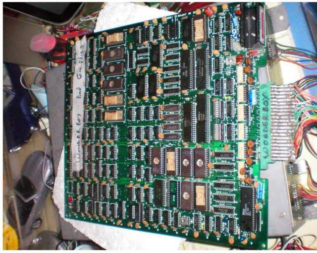
Firstly there was a ROM missing, secondly 2 of the ROMs were in the sockets the wrong way round, thirdly it obviously had Mitsubishi double-decker ROMs in the graphics section. I have never found one of these Mitsubishi ROMs that still works, most appear to be fine but contain gibberish, if you can manage to erase one fully (tricky) and reprogram it (trickier) it will probably only hold the data for an hour or so before the bits start dropping away. There was also tape across the back of the board which had "bad graphics" on it - probably due to the Mitsubishi chips.
When I got the board one of the Z80 had fallen out during transit and the remaining Z80 on the board had "BAD" written on it in marker pen.
There didn't seem much point powering it up as it was. The EPROMs in backwards were always likely to be toast and my reader confirmed this, shame really as they were decent chips and I am short of that size. I was hoping someone had taken them off to test and then just put them back wrongly, if they hadn't powered up the board they would have been ok. My tester also confirmed that the Mitsubishi M5l2764s were shot, they read ok but WinRomIdent didn't recognise them.
The remaining ROMs did read and dump OK but all of the ROMs in the main bank were in the wrong sockets. So I burnt new ROMs to fill the gaps, and put the working ROMs where they should be. I also had to made up a JAMMA adaptor for the board, a simple one initially that had the power, RGB, sync and speaker connections. I then powered it up - and got a totally blank black screen.
The board was getting power, the Z80s were getting clock and were not in RESET or HALT mode so I started probing around. I initially went for the RGB lines and sync and found I had nothing at all, not even sync. There was some activity on the board but generally it was very quiet. I tracked back from the RGB to a set of 3 resistor networks, one for each colour channel and confirmed that the input to the network was dead on each one, the inputs all went to the outputs on a couple of 74LS175s at IC07 and IC08...
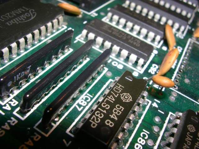
...which were always going to be doing nothing as their MR pin was held low, these were joined and tracked waaay back across the board to the Q (output) 74LS109 at IC69. These chips have 5 inputs, the RESET pin was tied high so the chip was active, the clock pin was getting a clock signal and the remaining pins (clear, J and K) were all tied together and attached to a track that went to a 7425 chip at IC90, this chip had pin 3 tied to 5volts via a current limiting resistor, pins 4 and 5 were also tied together which left pins 1 and 2 as inputs. These both went to custom chips, pin one to the 7114 PROM labelled PR5317 and pin 2 to a PAL with the Sega ID 315-5063, neither of which I could verify, but it looked rather like the video was not being initiated rather than there being a fault preventing it from working.
At this point it dawned on me that I was wasting my time as the board was probably missing something rather critical - the right CPU!!! I have fixed a couple of Wonderboys before but neither were quite as dead as this one, all had used stock Z80s so they arrived at my door with the unencrypted code already in the ROMs.
Sega originals usually used encrypted executable code, and to run that code you had to have the right CPU that contained extra circuitry that re-arrange the code before it was run on the CPU core, try to use a standard Z80 and it will crash because the ROMs contain gibberish as far as a normal CPU is concerned. This was to stop the operators from burning ROMs and upgrading the boards to a new game without throwing some coin to Sega. As they needed a hardware device (i.e. the right CPU) they had to pay for each game, copying your mates ROMs was pointless.
Luckily there is a decrypted version available for this board layout, Wonderboy came in a couple of variations in terms of ROM layout and the romset "wboyu" had the right layout for this board and only needed a few ROMs to be reprogrammed. As soon as this was done the board leapt into life, by the way the Z80 that had "BAD" written on it works perfectly so I don't know what that was about, perhaps a previous owner got the board after the CPU had been pinched, and only had one Z80 to test, thereby coming to the conclusion it was duff as it did nothing on the board. The death of the Mitsubishi EPROMs was probably the original fault, hence the masking tape message, and the CPU got pinched as a spare.
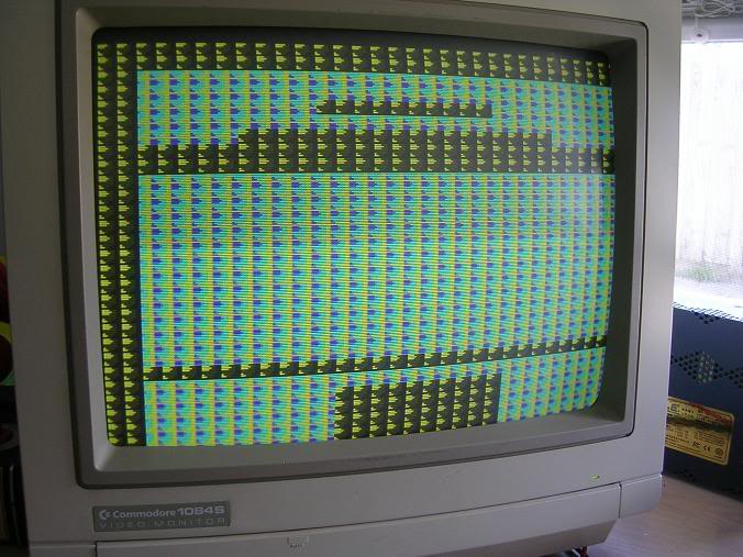
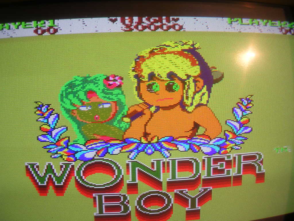
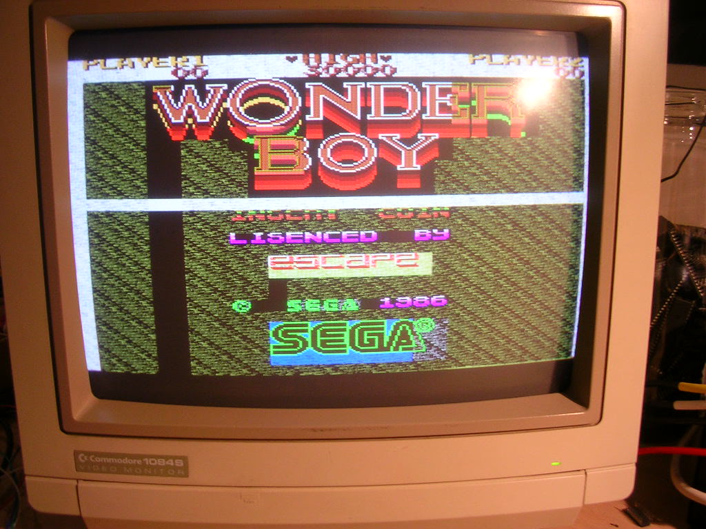
With correct code for a normal Z80 the game was now running but the title screen background was solid cyan, sometimes the whole screen..
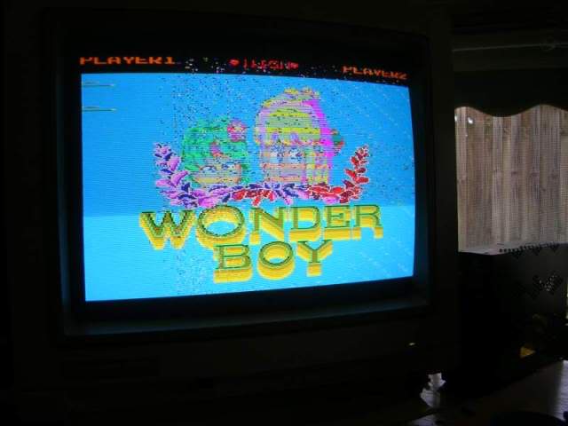
.. sometimes just a thick stripe down the middle of the screen.
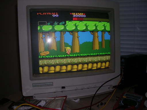
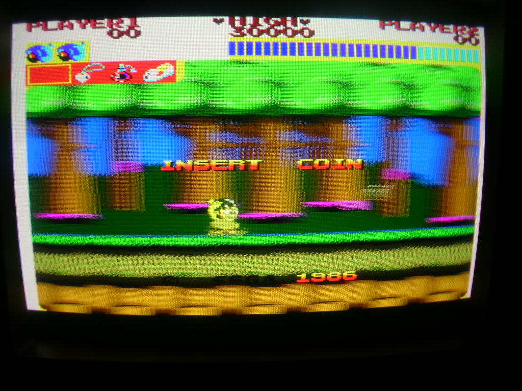
In the game things were much weirder, the colours where totally wrong for the in game graphics...
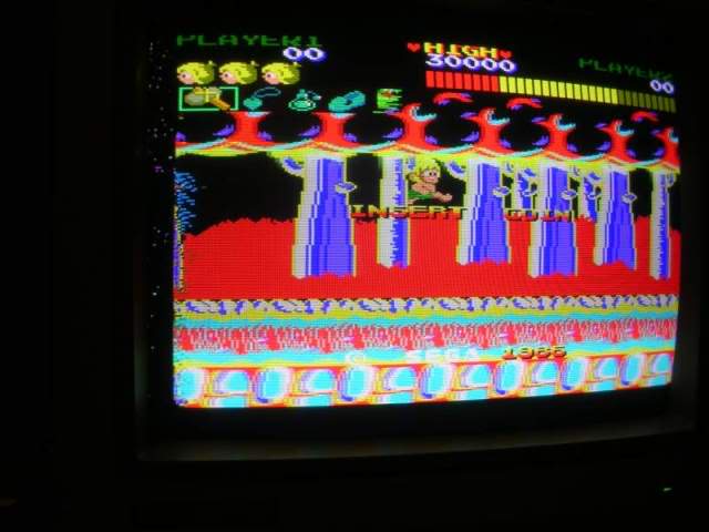
...so wrong it looked like the harness was wired up incorrectly, but the graphics for the health and life section of the screen were the correct colour.
The Wonderboy sprite was also a bit unstable, sometimes the "walking" sprite was torn up and only came good when he jumped or was on his skateboard. Probably the oddest issue was that the Wonderboy sprite was actually behind the background and was only visible when he jumped above the line of the red bushes or got out of the forest.
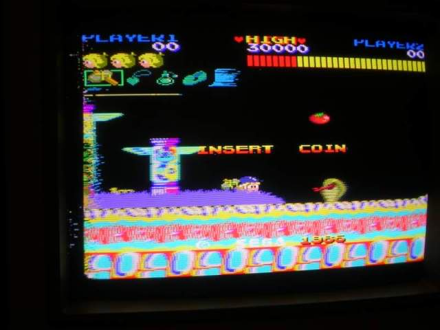
As the board has a smattering of Fujitsu TTL chips I started with those and found a couple of LS153s at IC9 and IC28 with missing outputs, when these were both replaced the background went black, better but it should be a beige colour.
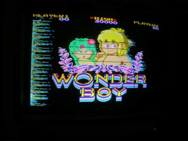
The final crazy colours and the "behind the background" issues were traced to an 74LS377 at IC19...
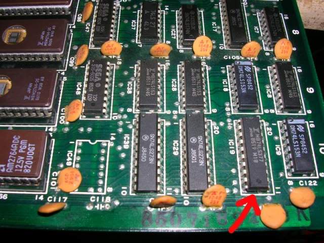
..again it was a Fujitsu chip but it didn't have the usual give-away missing output fault, it was just hyper sensitive to touch, when its pins were touched the Wonderboy sprite would totally mess up, often be drawn as a torn up mess of horizontal lines, irrespective of whether he was jumping or not, the splash screen did this...
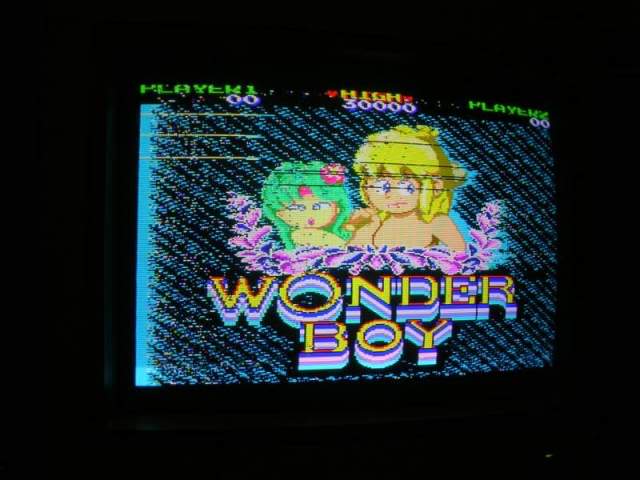
... which kinda gave away that the 377 was involved.
Replacing this chip had a dramatic effect, the colours of the landscape were suddenly correct, Wonderboy himself was back in the foreground again and rock solid again, the splash screen background was also the correct colour.
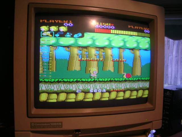
As the 377 and the pair of 153s were all in the same area of the board as 3 other Fujitsu 153s I replaced those too, nothing changed but those chips are almost certain to cause trouble in the near future so the board is better off without them.
At this point the game was almost perfect, the only remaining issue was that there was usually some lines of rubbish drawn on the screen down the left hand side, it seemed to come in 3 levels of "wrong". On some occasions the game would boot up and be perfect, on some occasions there were only a very few lines of crap but most of the time the rubbish was all down the left hand side.
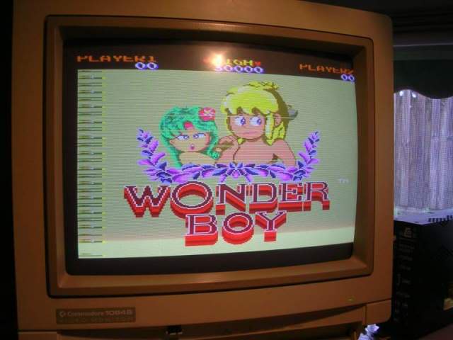
Whatever state I got when I booted the game was how it would stay until it was powered off, no matter how many times the screen display changed, something somewhere was getting stuck.
To be honest these sort of problems are the worst to troubleshoot, when are board does nothing the difference between it and a good board is very obvious. When a board does 99.99% the right thing and is only 0.01% wrong it can be almost impossible to spot where the fault is. Nothing showed up on the scope as being unusual, there were a couple of crappy Fujitsu 245s left to replace but any interruption to these crashed the board so they were unlikely to be involved with a graphics fault. The fault looked like something that happened extremely briefly when the board was powered up, the junk on the screen stayed present throughout the game and never changed, on power cycling the board it would be present in one of the three degrees of faulty, perfect, nearly perfect or full screen side of rubbish as in the last photo.
So I tested the smoothing caps across the power rails and they were all fine and had a poke around the reset system looking for anything that might be starting the board too soon, nothing stood out. So I started at the beginning, the ROMs, probing around the board I could not find a single area that affected the graphics artefacts, I could aggravate it in about 5 different regions of the board. So I started at the beginning, and pulled out the entire bank of 6 ROMs IC61 to IC66 and powered up the board. A lot of things were missing, and blocks of colour were gliding about the screen instead of the actual graphics, but the fault was still there, so those ROMs had nothing to do with it. The remaining 7 ROMs on the board (ignoring the sound CPU ROM) were the only place this junk could be coming from.
I didn't expect to get very far in pulling these out one by one as the main game code lives somewhere in that bank, if by pulling a ROM you take out a lump of the executable code you end up with a board that wont boot, which doesn't actually help much in isolating a minor fault. It turns out the at the game code only lives in the 1st EPROM and I hit the fault before I got that far, by removing the EPROM at IC110 the fault vanished, along with a the Wonderboy and Girl figures on the splash screen and some in game artefacts. The first thing to do was to replace the EPROM with another one to see if it was the chip itself. So I burnt a copy of the relevant data into a new 27C128 and dropped it in, the fault came back.
Buzzing round with the continuity tester I could see the data and address lines were connected up in a sane way with nothing missing.
The only thing left was the method of enabling the chip to output its data. On all EPROMs I have ever seen from the 80-90s arcade era there are two pins that control when the chip can "speak". Usually you have multiple chips sharing the same address bus and data bus, therefore all the chips in the stack hear which address location the CPU is asking for information from, and each chip has a location referenced by this address. Only one chip must be allowed to use the data bus at any given time, if you have more than one talker the data gets corrupted.
The high address lines on the CPU usually go into a logic system which selects which chip the CPU is actually wanting information from, the logic drags that EPROMs OE(output enable) pin and holds all the other ROMs OE pins high, the chip with the low OE pin is the only one that can speak. The other pin is actually a blanket enable pin, often called E or G depending on the manufacturer. This pin determines whether the EPROM is actually enabled, when it is logic high the chip is in a low power standby mode, when low the chip is active. Often these E pins are tied to ground so the chip is always enabled, it takes far longer for a chip to come out of its standby mode than it takes for it to be told to shut up via its OE pin so its not normally used as a way to control the chips on a running board when data is needed in a hurry.
On Wonderboy the E pin on IC110 is not grounded, it is actually connected to the E pin on the EPROM at IC117 and then it goes off to a 40 pin Sega custom IC called 351-5011 (which combined with the fat custom 5012 next door are system controllers according to Google, pinouts sadly I could not find), finding customs in a fault path is never good, there's no datasheets on what they do, no way to test them and usually no spares handy to do a straight swap. Pulling out IC117 didn't help the fault at all, it just removed more of the graphics data but the issue remained.
Anyway as the E pin is the less likely candidate for the fault I focused on the OE pin, which went off to a 74ls74 at IC06, this seemed to be doing the right thing on the scope, in fact the line was active and healthy looking, the fact that this fault only occurred at power on and then remained suggested that pretty much everything was fine except for a very brief period. The E pin is held low at all times anyway, its just controlled by the custom chip rather than being tied to ground.
At this point I ran out of puff, the board sat on the spare bed for a couple of weeks, I had already spent about 8 hours on it to this point and the custom chip kinda discouraged me.
When I finally got back to it I picked up where I left off and pointed a scope at the E pin, this did connect to pin 38 pin on the custom chip, plus the E pin on the EPROM at IC117 but it also went to the E pin on a 2148 SRAM at IC100. The outputs on this chip looked ok on the scope but it seemed plausible that it was failing in a way that meant it took longer to come out of disable mode, or that the combined load of the 2 EPROMs on the E line meant the signal to it was now borderline. It was a simple theory to test, desoldered the DRAM chip...
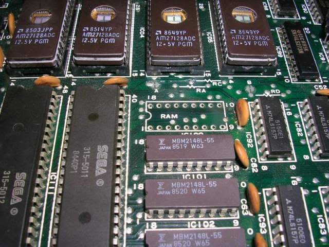
...grabbed one off the badly scrapped Wonderboy board I was given a while ago (sadly the custom chips had already been robbed from this one), fitted an 18 pin machined pin socket to the board and dropped in the chip.
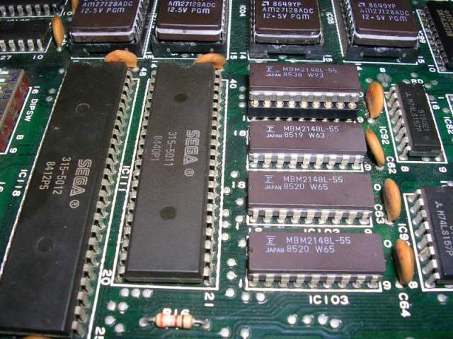
The fault was gone and stayed gone on subsequent reboots of the board, graphically the game was perfect again.
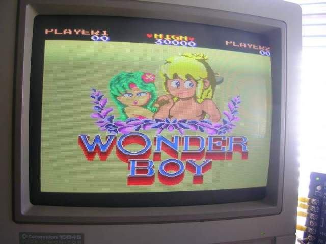
Next concern was that I still had not heard a single sound from the board. The JAMMA adaptor I had made had only the power, video and speaker wires connected, and the boards dipswitch was set to enable Demo Sound but it was silent. The amp seemed ok as I could introduce static by touching the underside of the board and its pins. Another issue was I could not set the game to free play either. I added the coin up and 1P start wires to the harness and started the game, and got sound, effects and music which confirmed the dipswitches were not working properly, mainly dipswitch bank B which handles attract mode sound and free play. These 8 dipswich blocks are often "read" by 74ls253 or 74ls257 chips on arcade boards, and these are known to die, presumably of boredom. On this PCB each bank had a 74LS257 connected up, both were Fujitsu chips. All of the outputs were active, but if an input had died this would explain the behaviour. I am now of the opinion that its not the chip core that dies on these Fujitsu TTLs but it is the microscopic wire from the pin to the pad on the chip core that fractures or corrodes away leaving pins disconnected. I took the pair of 257s off and tested them, , the 1st one was good but the one associated with dip bank B failed its test. When a couple of new (non Fujitsu) were put in it fixed the last issue, I can now set free play!
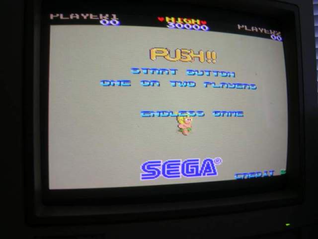
The game is finally fixed, only thing left to do is to print some labels for the EPROM chips! There are half a dozen Fujitsu TTLs left on the board, I will probably replace these in one shot, they will probably take down the board at some stage in the future, but for now she's healthy again
Board 2
Repairer: VectorGlow
Forum Thread: Wonderboy PCB Repair
As I've just repaired a Wonder Boy (single board, Sega original) with oodles of faults (it had 37 bad TTLs in total!) I thought it was worth posting my log files. I didn't document all of the faults, but most of them are here. Not in any way as detailed as womble's I'm afraid and no pics, but they should still be useful. Those nearer the end are for the original Sega type that has two daughterboards and a different layout.
Symptom: Horizontal lines through all sprites Cure: Stuck outputs on pins 4 and 7 of the LS157 at location IC58 (original Sega single board)
Symptom: All background tiles, text and graphics data (but not the sprites) is scrunched up very tightly and corrupted in the horizontal plane (original Sega single board) Cure: Dead outputs on the LS157 at location IC93
Symptom: No background being drawn except for a few random blocks (original Sega single board) Cure: Bad outputs on the LS157 at location IC72
Symptom: The whole display is scrolling vertically, some graphics and text visible, game won’t play (original Sega single board) Cure: Bad outputs on the LS669 at location IC79
Symptom: Display is just a scrolling herringbone pattern (original Sega single board) Cure: Bad socket for PROM PR-5317 at location IC7
Symptom: Assorted missing sync signals (original Sega single board) Cure: All outputs bad on the LS164 at location IC31
Symptom: No colour video output, only video sync. Game plays blind. Diagnosis and Cure: No clock inputs on pin 9 to the LS175’s at locations IC107, IC108 and the LS174’s at locations IC74 and IC74. This clock comes from pin 11 of the LS132 at location IC87, but the inputs to that were good AND replacing the chip didn’t help. Then noticed that the capacitor at location C123 (just below IC87) had a 0.1uf cap in place – replacing that cap with a 220pf cap fixed the fault. Only knew that this was a 220pf cap from referring to a known good board, which had the cap code of ‘221’. Note: Removing the cap brought back the video, but caused intermittent horizontal bleeding ‘streaks’ of yellow extending from the right of all sprites. Replacing it of course fixed that issue too.
Symptom: Using the Fluke, test main or sprite RAM – there’s a R/W Error at the starting address BTS 40 (original Sega single board) Cure: Bad LS245 at location IC125
Symptom: Two characters on the title screen are incomplete and partly ‘smeared’ (original Sega single board) Cure: Broken track between pins 19 of the 27128 EPROMs at locations IC104 and IC105, so there was no connection to pin 3 of the LS273 at location IC99
Symptom: No background tiles, only sprites and a few bits of rubbish (original Sega single board) Cure: Bad LS157 at location IC71
Symptom: Variable “phut phut phut” sound from the speak which is of the same volume irrespective of the pot setting, no other sounds Cure: Bad LS4460N amp
Symptom: Sprites badly positioned and flickering on and off, plus badly broken up (original Sega single board) Cure: The four LS157’s at location IC52, IC53, IC57 and IC58 all had faulty outputs
Symptom: Screen is showing assorted short-ish, flickering horizontal lines. Also, the bottom quarter of the display is displayed four times, filling the screen (original Sega single board) Cure: Bad outputs on the LS157 at location IC71
Symptom: Some of the colour shades missing, especially red (original Sega single board) Cure: Some dodgy outputs on the LS175 at location IC108
Symptom: No video sync (original Sega single board) Cure: bad output on pin 11 of the LS86 at location IC10
Symptom: Vertical scrolling is very jerky, bottom half of screen reproduced at the top during gameplay – no clock on pin 11 of the LS374 at location IC03 (original Sega single board) – a similar fault can also be caused by this actual LS374 being at fault, shown as the lower part of the screen being too high (Wonder Boy sprite half hidden behind it) and when the ground angles upwards it’s also drawn too high – in this case caused by the output on pin 6 being stuck High Cure: Bad output on pin 12 of the LS157 at location IC71
Symptom: Vertical scrolling not working (original Sega single board) Cure: Bad outputs on the LS273 at location IC03
Symptom: Some colours wrong (original Sega single board) Cure: Bad LS153 at location IC9
Symptom: No sprites (original Sega single board) Cure: Bad LS244’s at locations IC2 and IC3
Symptom: Display split in half horizontally, just the two right halves doubled up (original Sega single board) Cure: Bad LS283 at location IC40
Symptom: On power up, ‘WONDER BOY’ text split horizontally and high scores too spread out (original Sega single board) Cure: Bad LS283 at location IC50 Symptom: Text, graphics, etc all consists of short, thick, vertical lines (original Sega single board) Cure: Bad LS283 at location IC01
Symptom: Only the base of the screen is drawn, multiple times (original Sega single board) Cure: Bad LS157 at location IC72
Symptom: All text and graphics repeated vertically eight times (original Sega single board) Cure: Bad LS157 at location IC83
Symptom: Sprites displaying incorrectly (original Sega board with daughterboards) Cure: Output pins 5 and 6 not toggling on LS74 on the Sprites daughterboard, bad outputs as inputs good
Symptom: Colours wrong (original Sega board with daughterboards) Cure: Combination of a bad 6116 RAM chip at location IC151 and a bad LS175 at location IC152
Symptom: No sound (original Sega board with daughterboards) Cure: Combination of a bad 6116 RAM chip at location IC7 and a bad LA4460 sound amp, both replaced and sound working fine
Symptom: Background partly garbled, no black areas where they should be at the top of the screen and other faults (original Sega board with daughterboards) Cure: Bad 6116 RAM at location IC102 - replaced
Symptom: The ground is broken up, looks like there’s been an earthquake, some segments a bit higher than others, the layout of the broken segments varies from game to game. Also occasional thick vertical black bars above the ground are, plus some background graphics corruption, such as random bits of other graphics in the totem poles in the third section of the first level (original Sega board with daughterboards) Cure: One poorly seated chip in program EPROM sockets 1 – 6 but not sure which one!
Symptom: Vertical scrolling and positioning messed up, for example on the title screen the red WONDER BOY text scrolls up very jerkily and ends up too high (positioned behind Wonder Boy and his girl) plus that same text is split horizontally down the middle with a large gap between the two halves. Also affected by this fault is the vertical scrolling of the high scores which is also jerky and mis-placed. Finally, the in-game ground graphics are duplicated vertically so obscuring the main character, etc. (original Sega board with daughterboards) Cure: Bad 74LS283 at location IC6 on the 834-5541 daughterboard (Additional: had a similar problem occur a few hours after fixing this one which turned out to be the other LS283 (location IC7) on the same daughterboard – in this case though the scrolling was less jerky and the Wonder Boy text only ended up a little higher than it should have been)
Symptom: All graphics, including text, cut in half and roughly doubled horizontally (original Sega board with daughterboards) Diagnosis: Found that grounding pin 3 of the LS368 at location 1U caused the problem to be resolved. Replaced the 368 but fault remained. Traced pin 3 (an output) to the LS283 at location 1S, piggy-backed a good LS283 on the existing one and the fault went away. Cure: Replaced LS283 at location 1S
Symptom: All sprites are a thin vertical line, or not visible at all (original Sega board with daughterboards) Cure: Bad outputs on the LS175 at location IC91, particularly pin 3
Symptom: Thin horizontal lines through all sprites. Also some of the background. Plus thin vertical lines on the left half of the display (original Sega board with daughterboards) Cure: Bad output on pin 6 of the HC32 at location IC11
Symptom: Most colours non-existent, all that’s displayed are shades of a yellowy-green and an off white for the text (original Sega board with daughterboards) Cure: Bad LS245 at location IC150
Symptom: Screen display doubled vertically (original Sega board with daughterboards) Cure: Bad output on pin 9 of the LS157 at location IC2 on the 834-5541 daughterboard
Symptom: Screen display doubled horizontally (original Sega board with daughterboards) Cure: Bad output on all relevant pins of the LS157 at location IC1 on the 834-5541 daughterboard
Symptom: No blue (original Sega board with daughterboards) Cure: Pin 11 of the LS175 at location IC152 was stuck high internally and no output from pin 10 – replaced IC
Symptom: Vertical scrolling not working at all, loads of short horizontal dashes flickering all over the display AND the dashes were additionally being drawn in the overscan areas. (original Sega board with daughterboards) Cure: Bad LS245 at location IC5 on the 834-5541 daughterboard
Symptom: Sprites problem – for example, on the title screen with Wonder Boy and Tina, Tina is a smeared, horizontally stretched mass of pixels, and some in-game sprites are similarly smeared. (original Sega board with daughterboards) Cure: Bad LS245 at location IC108 – replaced
Board 3
Repairer: Womble
Forum Thread: Wonderboy PCB Repair
Have had some success repairing boards of late, one of my victories has been a Wonderboy.
The game landed on my desk with an odd fault. All sprites and icons were totally missing, the splash screen icons were all the wrong colour and the border was beige instead of black. Other than that it was great
Someone had previously removed IC74 at 8M (an LS174), they had fitted a machine pinned socket and used half a reel of solder and a whole can of lacquer in the process. It was a globby mess, to rule out shorts I had to remove the lot. The IC tested ok so it was soldered in directly. One track didn't survive the process so a link wire was fitted. This didn't cure anything, but at least the board wasn't a mess.
I initially was certain that the missing sprites would be a RAM problem, I was wrong, all ram lines were busy, and piggy backing known good RAM changed nothing. So I went over the board with the logic probe.
Found an 74LS04 at 1N(IC97) had a floating output pin, piggybacking a new chip on it lit up the line and instantly restored the sprites. The old chip was binned and the new one soldered directly in.
The border was still beige and the freeplay splash screen sprite was blue, I could find no other missing pins, other than ones that could be explained by their datasheets (either not connected, or unused input pins on hex or quad chips).
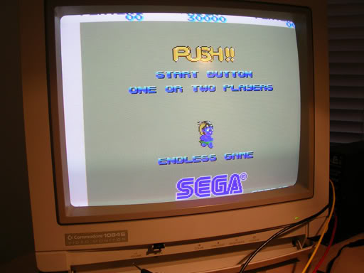
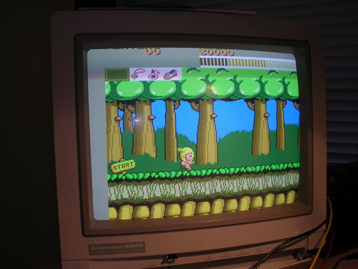
Finally found an LS157 at L10 (IC77) that when piggybacked made the start screen go nuts. Turns out that piggy backing on that chip will only take effect from a cold start. Chopped it out, soldered in the new one and the game is now 100% fixed.
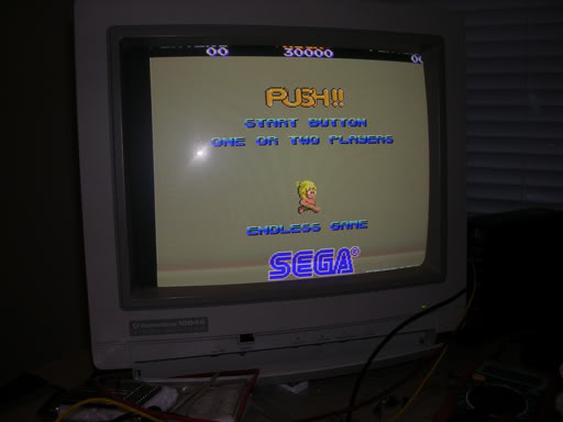
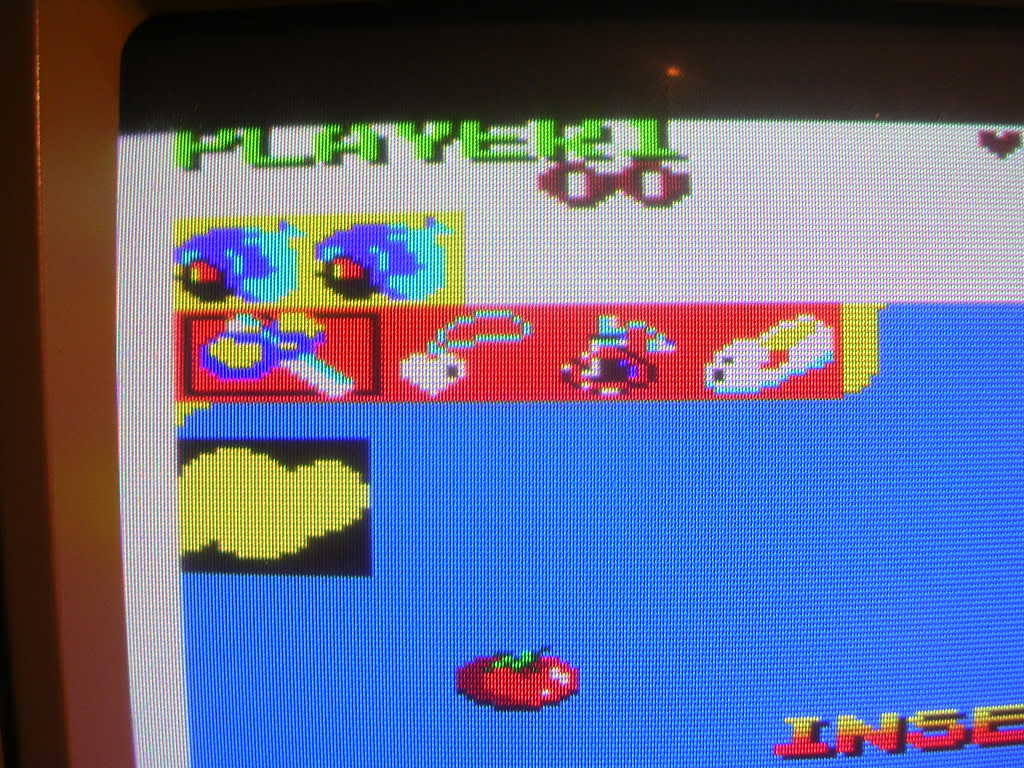
The large black space in the top left is where the lives remaining icons go, the board was set to free play so nothing shows up there until you find a extra life powerup. When not in freeplay that area has the 4 faces for the 4 lives.
The only problem now is that my wife keeps wanting to play it.
Board 4
Repairer: Womble
Forum Thread: Wonderboy PCB Repair
Another Sega Wonderboy PCB saved from the scrap bin.
Problem - garbled graphics, game runs but everything except the sprites is scrambled.
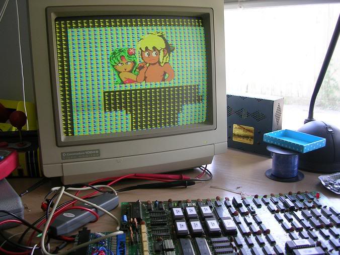
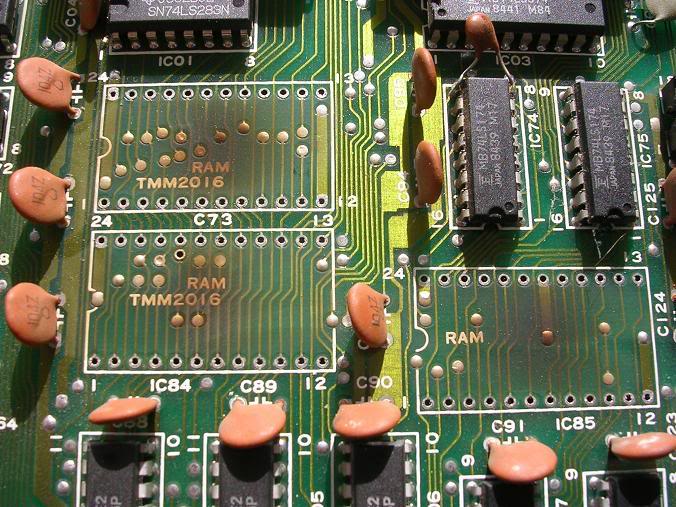
Fired it up, checked the RAM outputs with the logic probe, everything that should show activity was active. So moved onto the logic, and after 2 or 3 minutes burnt my arm on the RAM chips, these 3 were stinking hot. The 4th chip to the bottom left of the trio was barely warm to the touch.
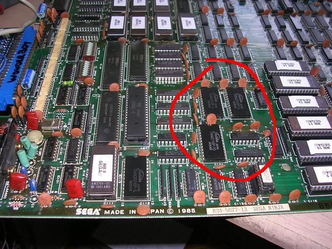
Unsoldered them and it became clear how hot these had been getting, the board under each of them is pretty scorched, this board must have been left to cook for quite a while.
Cleared up the charring as best I could with PCB cleaner, didn't make a huge difference tho, fitted sockets, dropped in 3 salvaged 6116 chips and fired it up.
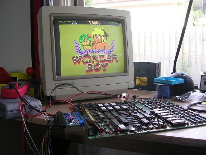
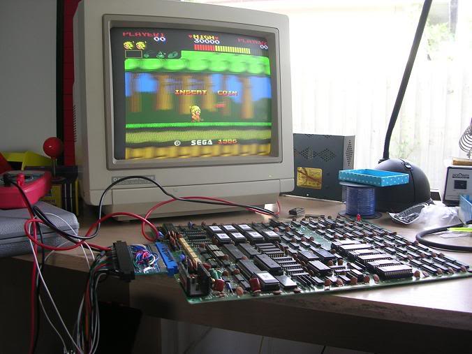
One happy Wonderboy PCB
One more board left to fix - that one has everything ok except the enemy sprites are totally missing. Logic weirdy somewhere I would think.
Board 5
Repairer: Womble
Forum Thread: Wonderboy PCB Repair
Had Gt-rays Wonderboy in for some TLC recently.
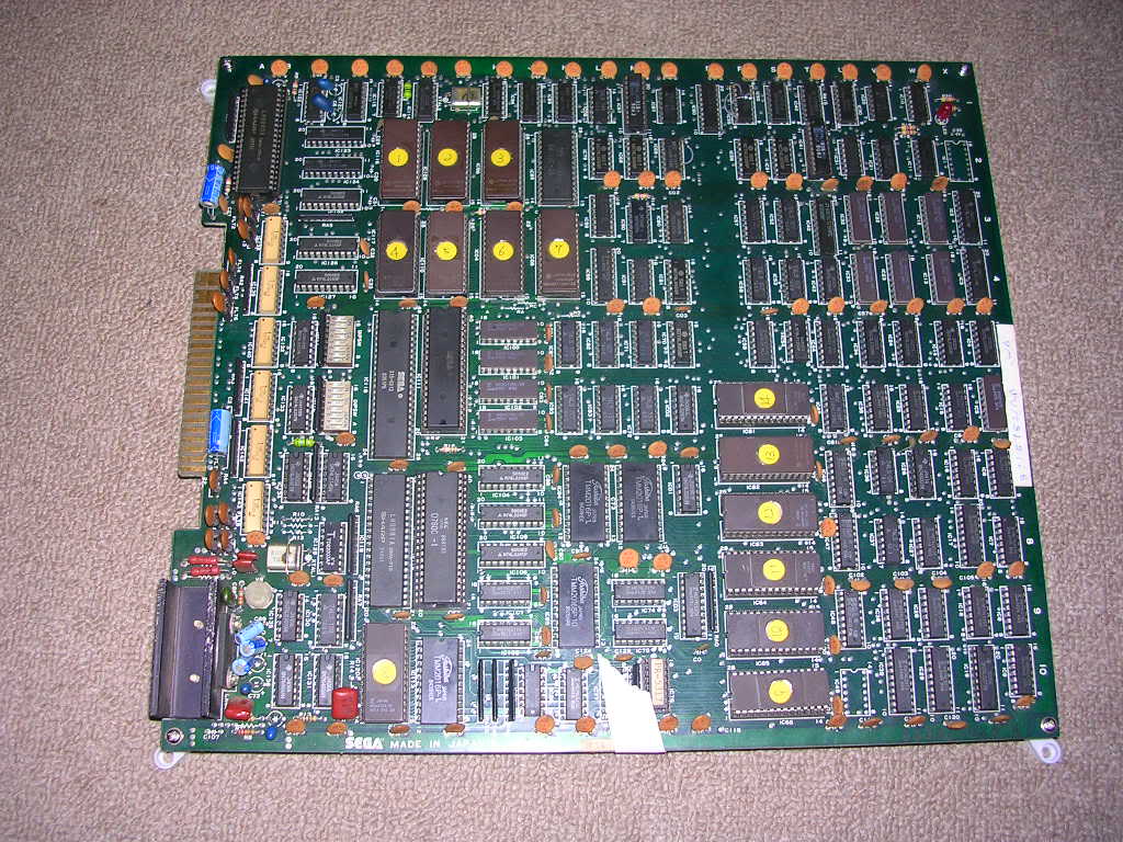
The board was in good nick, a couple of chips had been replaced by Gt-ray himself in an attempt to fix the board. The chips replaced were ones I had found to be faulty in previous repairs. This approach is not likely to lead to success as there are many chips involved in any single thing you see on the screen, so even if the fault is similar the chances the exact same chip is the cause is pretty low.
Aside from those chips there was this at IC55 and IC69...
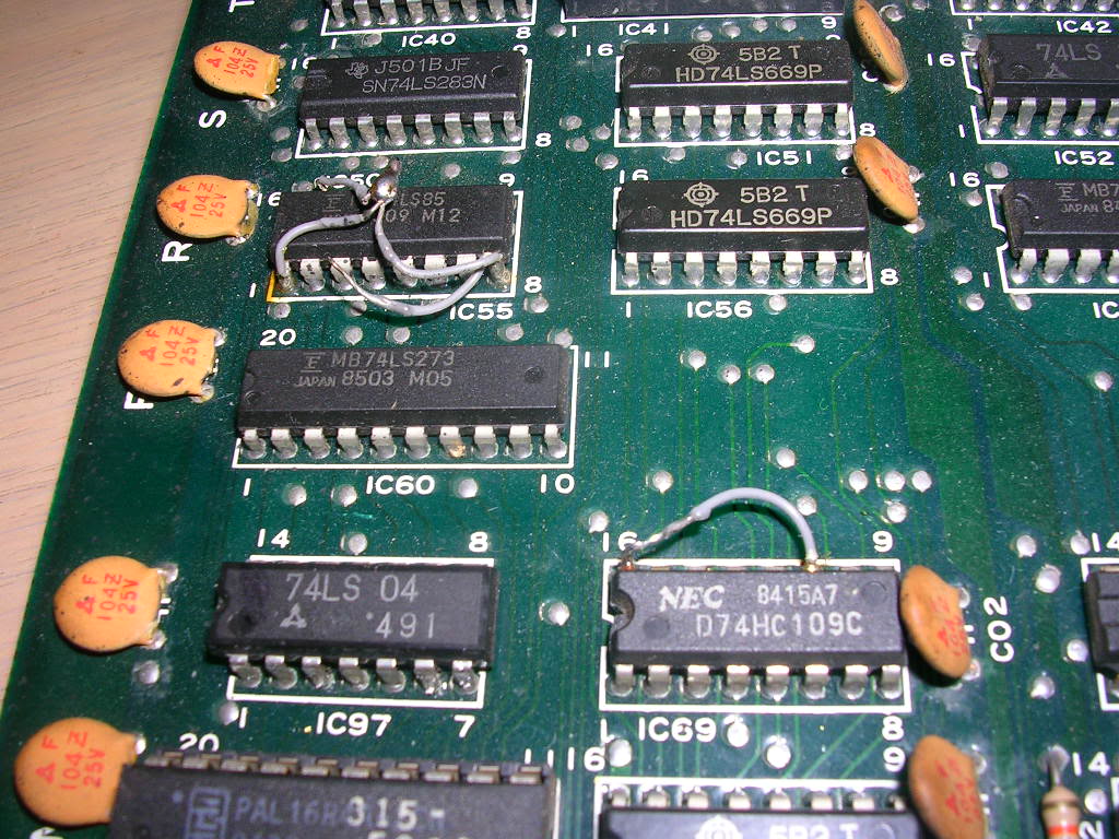
...little links of burnt wire badly soldered across a couple of chips - very odd.
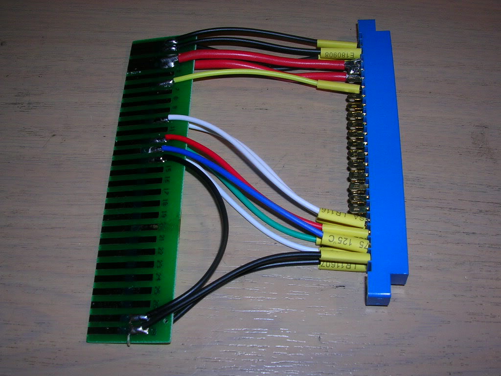
As I had foolishly sold my Sega System 2 adaptor with my last Wonderboy board I had to make up another one to even power this up, a very tedious job, this one isn't going anywhere as I hate making up these things. It's such a dull job that I only wired up the power lines, the video and the sound at this stage, enough to power up the board and see what it does.
As expected, it was not well...
... aside from the messed up colours which seemed to change at random, the screen was very glitchy and covered with noise from time to time.
First thing to do was to undo the crazyness on the LS85.
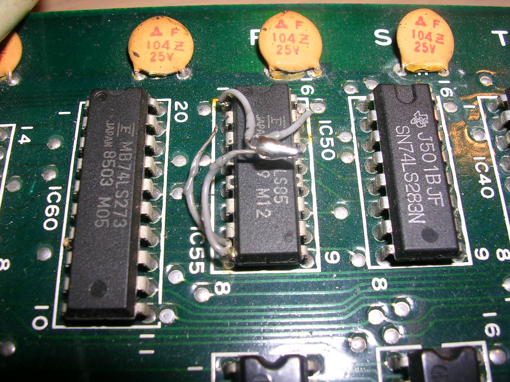
I had assumed that this was to connect up an unused gate on the chip to take over from a bad gate that the PCB connected to. Often TTL chips contain the same gate two, four or six times and in many cases the board doesn't use them all. However this wiring makes no sense whatsoever as the chip is a 74LS85, a single device and tying these lines together is going to bugger up the function of the chip entirely by joining four input lines to ground, (actually only 3 as one of the wires was just not actually soldered to anything on one end).
After trying to see any sense in what had been done I simply removed the chip and the bits of wire, fully expecting to find the chip was bad. Except it wasn't, my VP280 EPROM reader gave the LS85 a clean bill of health, and despite it being a Fujitsu TTL chip it went back on the board. 74LS85s are not common chips on arcade boards and I couldn't find a single one in my scrap PCB bin. The game was such a mess and so unstable when running that I couldn't actually tell if this had made any difference at all.
I had a poke around the video mixer section of the board with the scope and didn't find anything that looked bad, but as there were a collection of Fujitsu 74LS153 multiplexer chips in that area I fired up the HP 10529A logic comparator to compare a known good ls153 with the ones on the board. Due to the complexity of the 153 (12 input data streams producing 2 outputs data streams) it is impossible to see if it is doing the right thing with a scope, or a logic probe. As long as the output signal looks healthy you have no way to tell if the actual data it represents is bad, without feeding the same inputs to a known good chip and comparing the outputs to the on-board chip - which is exactly what this device does.
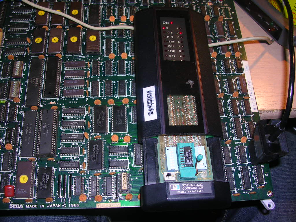
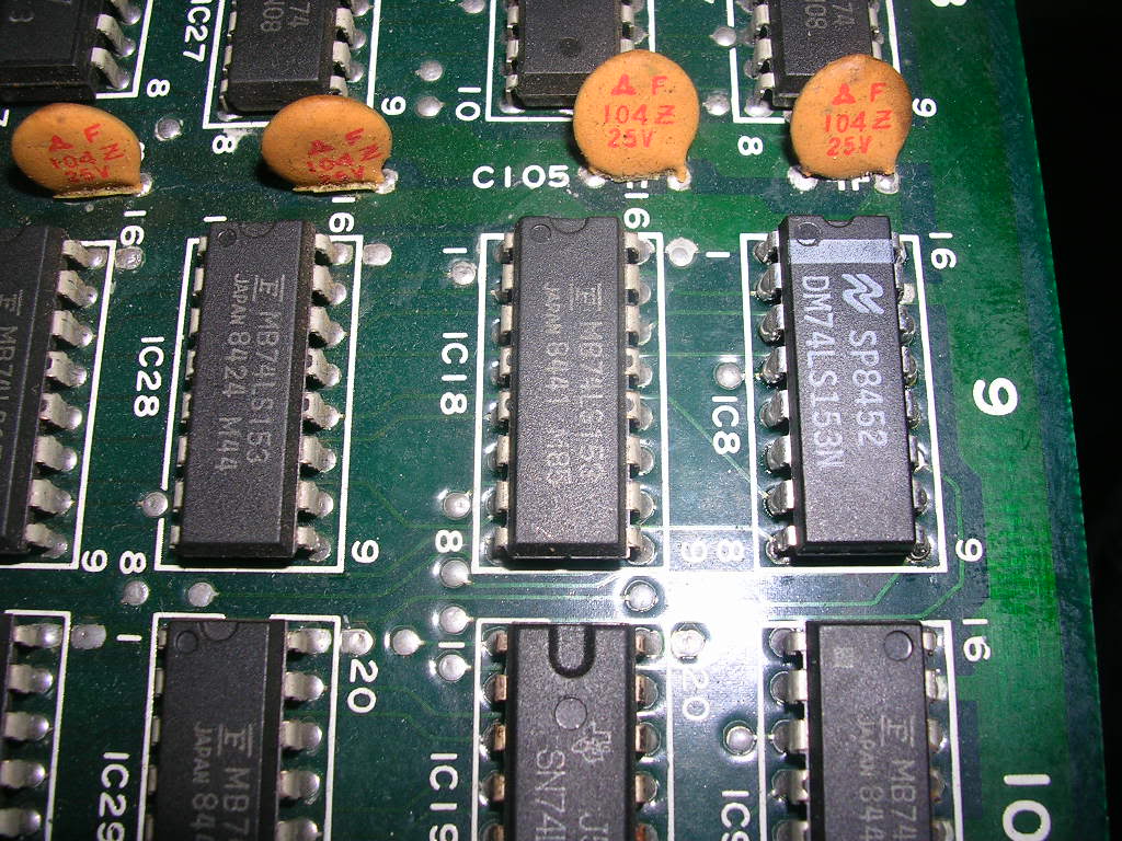
The LS153 at IC8 was bad, giving a constant mismatch between it and a good chip. So this was de-soldered and a good one soldered in its place.
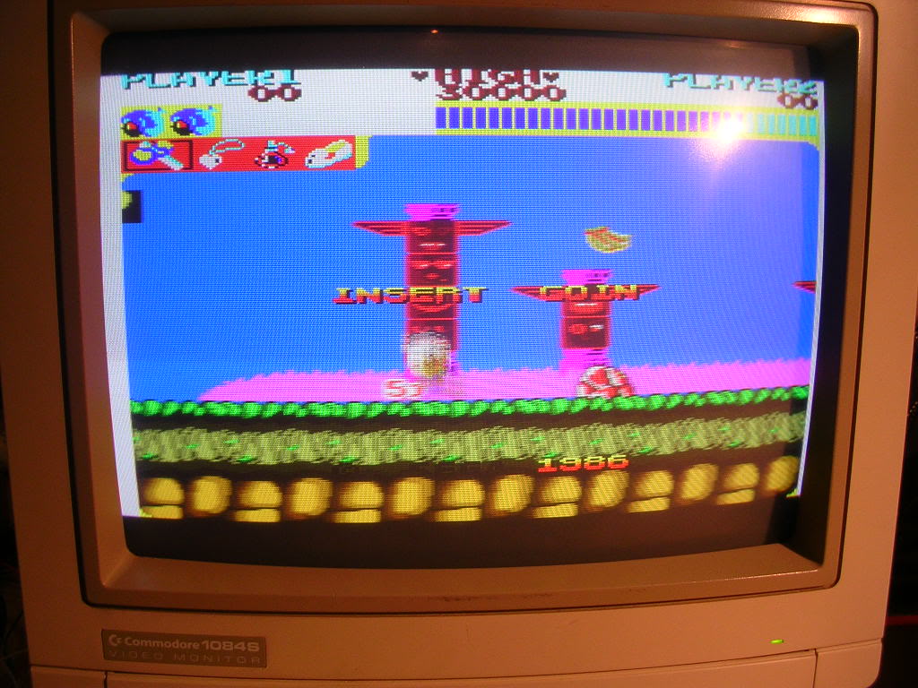
Firing up the board again gave this...
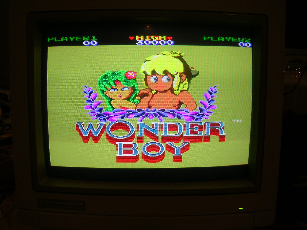
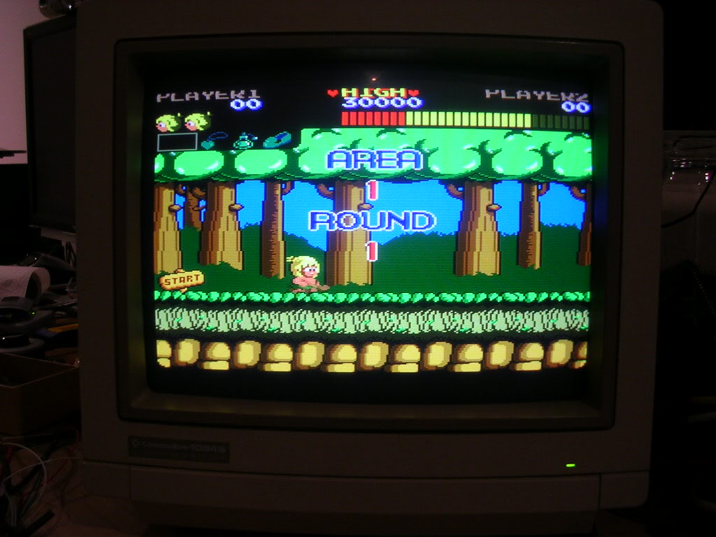
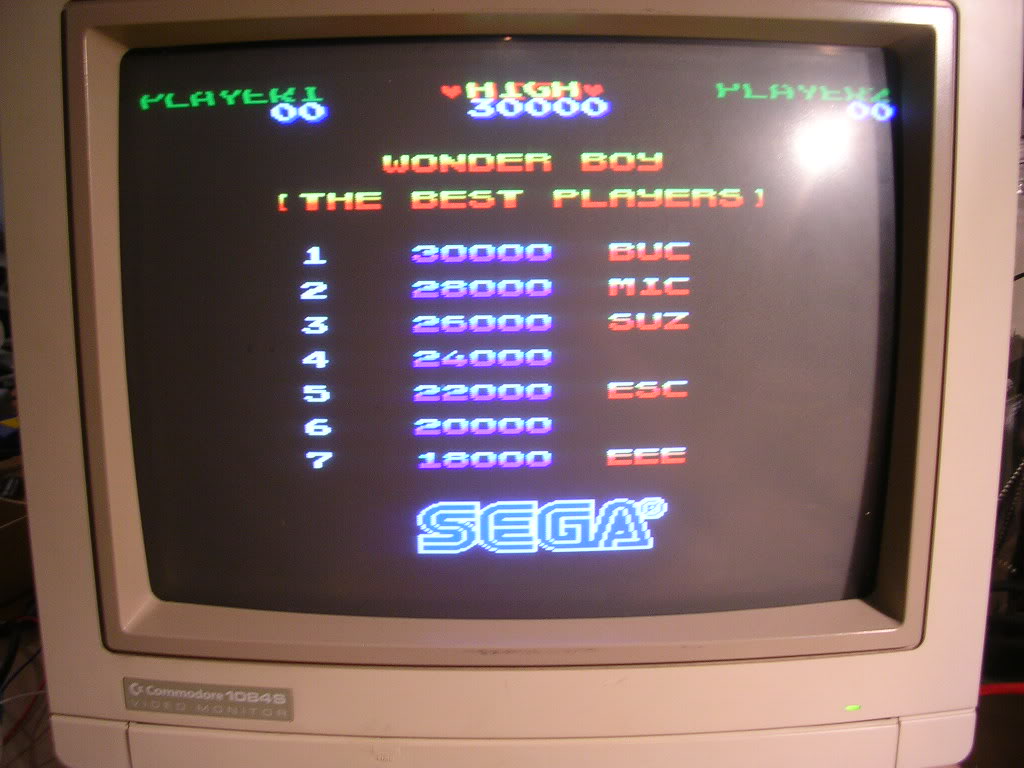
... and no glitching or flashing either.
As the board was back in good health I removed the weird wire link on the the 74HS109 chip to see what affect it would have - absolutely nothing, so it stayed off.
I have seen some shotgun repair attempts before but usually that just involves replacing chips semi randomly, this is the first time I have seen evidence of what I can only assume is someone going over the board shorting things together and seeing if it makes things better or worse, if it seems to improve things then they wire in a link in and carry on.
If anyone can suggest any more logical suggestion I would be interested to hear it as my explanation is hard to believe.
Last thing to do was to wire in the 8 player 1 control wires (Coin, Start, Up, Down, Left, Right, Fire, Jump) into the harness to confirm the board was actually playable and I ran through the first four stages without any issues at all.
Another Wonderboy fixed!
