PCB Repair Logs Pacman 2 1
Pacman 2 in 1 (Bootleg)
Repairer: Arcade King
Forum Thread: Pacman 2 in 1 PCB Repair
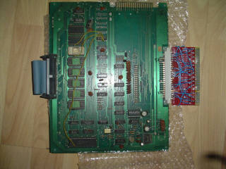
This was the pic of the board on the E-bay, Chris the guy who won it paid I think like 95 pounds for it or something.
Notice the Jamma adapter, it magically went missing when I picked up the board off JP.
Before we start
SBC=Sync Bus Controller
VRA=VRAM Addresser
The sync bus controller interfaces the external devices to the processor. The address and data bus are connected to the roms directly, but for ram and IO port access the sync bus controller gets in the way. An important thing to note is that the 6M* input to the SBC trails the 6Mhz used to generate the timing clocks by 1/3 phase, so the edge occurs during each level of 1H. The /CS line is asserted during a /MREQ with A14 high, during a non-refresh cycle (/RFSH high).
To handle interrupts, Pacman uses the I interrupt regiester to store the high 8 bits of the interrupt vector address and writes the low 8 bits to 0x00, which stores it in the register at U7.
During a mode 0 interrupt, /IORQ and /M1 are asserted, and the stored value is put back onto the data bus, and used as the low 8 bits of the of interrupt vector.
