Difference between revisions of "PCB Repair Logs Wardner"
m |
m |
||
| (2 intermediate revisions by the same user not shown) | |||
| Line 4: | Line 4: | ||
<tr class="> | <tr class="> | ||
<td colspan="2" class="" style="text-align:center;">[[Image:marquee_wardner.jpg|200px]]</td> | <td colspan="2" class="" style="text-align:center;">[[Image:marquee_wardner.jpg|200px]]</td> | ||
</tr> | |||
<tr class=""> | |||
<th scope="row" style="text-align:left; white-space: nowrap;">Manufacturer</th> | |||
<td class="" style="">[[PCB_Manufacturers_Taito|Taito]]</td> | |||
</tr> | |||
<tr class=""> | |||
<th scope="row" style="text-align:left; white-space: nowrap;">Year</th> | |||
<td class="" style="">1987</td> | |||
</tr> | </tr> | ||
<tr class=""> | <tr class=""> | ||
| Line 11: | Line 19: | ||
<tr class=""> | <tr class=""> | ||
<th scope="row" style="text-align:left; white-space: nowrap;">Pin Out</th> | <th scope="row" style="text-align:left; white-space: nowrap;">Pin Out</th> | ||
<td class="" style=""> | <td class="" style="">[[PCB_Pinouts_Jamma|Jamma]]</td> | ||
</tr> | </tr> | ||
| Line 25: | Line 33: | ||
<br> | <br> | ||
...the first one I fired up did nothing, just a blank screen. Turns out it was a very quick fix, one of the custom chips at E5 (labelled WTC02) was socketed and a slight shadow on one pin mad it look like it was bent under, so I took it off to check, all the pins were fine but I found this... | ...the first one I fired up did nothing, just a blank screen. Turns out it was a very quick fix, one of the custom chips at E5 (labelled WTC02) was socketed and a slight shadow on one pin mad it look like it was bent under, so I took it off to check, all the pins were fine but I found this... | ||
<br> | |||
<br> | |||
[[File:Pcb repair wardner 2 1.jpg]] | |||
<br> | |||
<br> | |||
... someone had slipped when levering the chip out and had not only smashed the socket but ploughed a lump out of the board, which had clearly broken a track to a pin from the via. I could beep through from the torn end of the track to the nearest pin, I could probably have guessed it was that pin but this way I was sure and didn't have to take the socket off. | ... someone had slipped when levering the chip out and had not only smashed the socket but ploughed a lump out of the board, which had clearly broken a track to a pin from the via. I could beep through from the torn end of the track to the nearest pin, I could probably have guessed it was that pin but this way I was sure and didn't have to take the socket off. | ||
So a 1cm length of hookup wire soldered in place bridged the gap... | So a 1cm length of hookup wire soldered in place bridged the gap... | ||
<br> | |||
<br> | |||
[[File:Pcb repair wardner 2 2.jpg]] | |||
<br> | |||
<br> | |||
... and the board booted up and ran. | ... and the board booted up and ran. | ||
<br> | |||
<br> | |||
[[File:Pcb repair wardner 2 3.jpg]] | |||
<br> | |||
<br> | |||
[[File:Pcb repair wardner 2 4.jpg]] | |||
<br> | |||
<br> | |||
The colours were not right, the blue channel was missing from the RGB out. I could see the colour signals leaving the JAMMA connector on the red, green and sync lines but the blue line was silent. | The colours were not right, the blue channel was missing from the RGB out. I could see the colour signals leaving the JAMMA connector on the red, green and sync lines but the blue line was silent. | ||
When the board was powered down I could trace the blue track back to a block of resistors which were fed by a couple of 74ls273, all of which looked fine on the scope. Heading back along the blue track towards the JAMMA connector there was a via which was a handy point to probe, it too looked fine. There was a healthy looking track between the via and the edge connector and when I pressed the probe hard into the blue pad I got a signal, turns out the fault was just a pretty oxidised JAMMA connector, a quick going over with metal polish and the blue signal reappeared. | When the board was powered down I could trace the blue track back to a block of resistors which were fed by a couple of 74ls273, all of which looked fine on the scope. Heading back along the blue track towards the JAMMA connector there was a via which was a handy point to probe, it too looked fine. There was a healthy looking track between the via and the edge connector and when I pressed the probe hard into the blue pad I got a signal, turns out the fault was just a pretty oxidised JAMMA connector, a quick going over with metal polish and the blue signal reappeared. | ||
<br> | |||
<br> | |||
[[File:Pcb repair wardner 2 5.jpg]] | |||
<br> | |||
<br> | |||
[[File:Pcb repair wardner 2 6.jpg]] | |||
<br> | |||
<br> | |||
Board fixed! | Board fixed! | ||
<br> | <br> | ||
<br>[[PCB_Repair_Index|Back to PCB Repair Index]] | <br>[[PCB_Repair_Index|Back to PCB Repair Index]] | ||
Latest revision as of 10:29, 7 February 2013
Wardner
 |
|
| Manufacturer | Taito |
|---|---|
| Year | 1987 |
| PCB Image | Wardner PCB |
| Pin Out | Jamma |
Repairer: Womble
Forum Thread: Wardner PCB Repair
Got a pile of boards from Left_jump_left_1P's, three of which were original Taito Wardner boards...
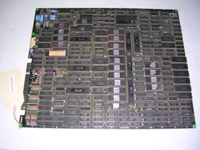
...the first one I fired up did nothing, just a blank screen. Turns out it was a very quick fix, one of the custom chips at E5 (labelled WTC02) was socketed and a slight shadow on one pin mad it look like it was bent under, so I took it off to check, all the pins were fine but I found this...
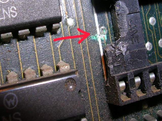
... someone had slipped when levering the chip out and had not only smashed the socket but ploughed a lump out of the board, which had clearly broken a track to a pin from the via. I could beep through from the torn end of the track to the nearest pin, I could probably have guessed it was that pin but this way I was sure and didn't have to take the socket off.
So a 1cm length of hookup wire soldered in place bridged the gap...
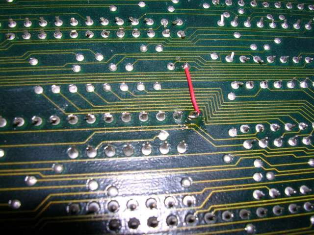
... and the board booted up and ran.
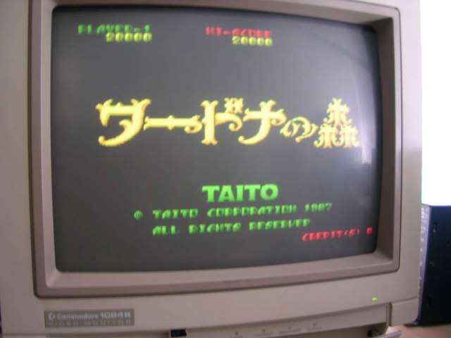
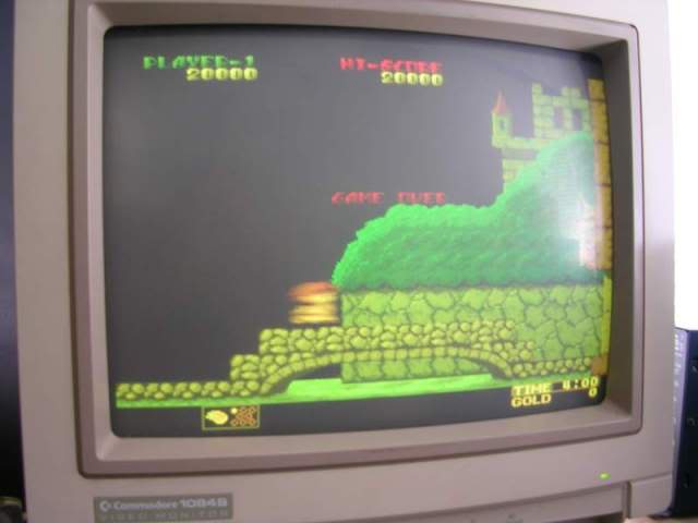
The colours were not right, the blue channel was missing from the RGB out. I could see the colour signals leaving the JAMMA connector on the red, green and sync lines but the blue line was silent.
When the board was powered down I could trace the blue track back to a block of resistors which were fed by a couple of 74ls273, all of which looked fine on the scope. Heading back along the blue track towards the JAMMA connector there was a via which was a handy point to probe, it too looked fine. There was a healthy looking track between the via and the edge connector and when I pressed the probe hard into the blue pad I got a signal, turns out the fault was just a pretty oxidised JAMMA connector, a quick going over with metal polish and the blue signal reappeared.
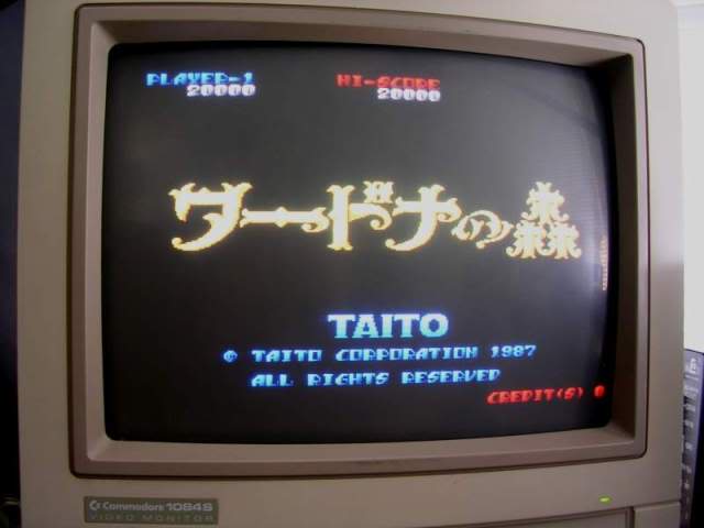
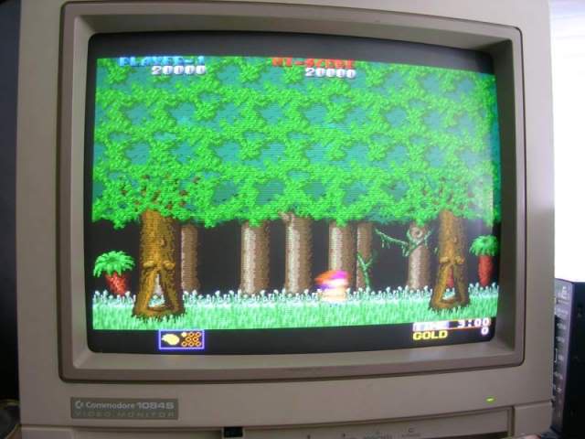
Board fixed!