PCB Repair Logs Neo Geo 6 Slot
Neo Geo 6 Slot
 |
|
| PCB Image | Reserved |
|---|---|
| Pin Out | Reserved |
Repairer: Womble
Forum Thread: Neo Geo 6 Slot PCB Repair
Had Scratcha's NeoGeo 6 Slot on the bench today, fricken massive thing but unwell, it booted up giving this RAM error..
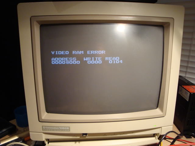
These error messages can be read like this...
The board tried to write XXYY to the two ram chips in the memory stack at the location stated, XX to the low addressed chip and YY to the high addressed chip (or perhaps the otherway round, it doesn't really matter). So from the above error you can infer that both chips are faulty, but only if you assume that its not a problem in the RAM controller logic, which is also possible. NeoGeo boards have an onboard battery that leaks corrosive shite when they age and the tracks on these boards are microscopic, they don't like the battery acid and they just corrode away to dust, track damage is a common problem.
The second problem with NeoGeo boards is finding which RAM chips the error message is talking about, half the problem there are so many board variants so chip location advice you find for a 2 slot board is not much use for a 4, or even a 6.
Anyway - with a bit of googling I found that the address the error message refers to determines which chip type is considered faulty.
Address 0000 means the board thinks the surface mount 62256 RAM chips are the problem, if that was the error for this board I would consider it scrap, or a boat anchor, its big enough.
Thankfully this error was at address 8000 which meant it was the Sony CKX5814 chip pair in the top right-hand corner of the lower board. It also helped that my logic probe showed the lower of the pair had its I/O lines D3 to D7 stuck low. The other chip looked healthy based on pin activity alone.
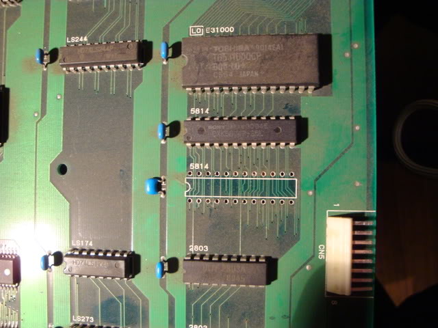
Desoldered this chip and tested on my eprom burner/chip tester and it showed up as faulty. Comparing the datasheets for this chip and the chips I had on my scrap boards showed I could use bog standard 6116 chips as replacements, so I dropped one in and fired the board back up to see what the error message would give.
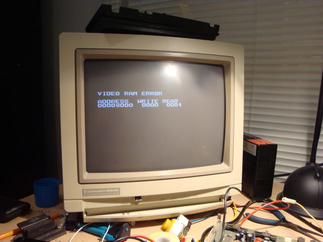
So now the board is writing 00 to one chip and getting 00 back, but still writing 00 but getting 04 back from the second chip in the pair.
Replaced the second chip (which also tested as faulty) and the board booted to the crosshatch screen, which is what a NeoGeo board should do without a game cart inserted, or in this case without the cart interface board connected.
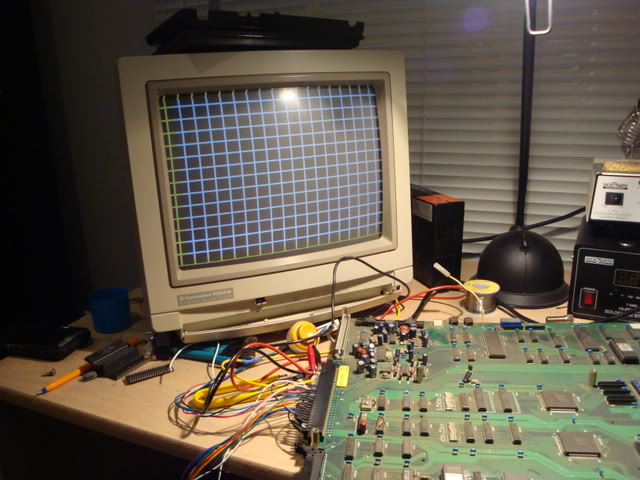
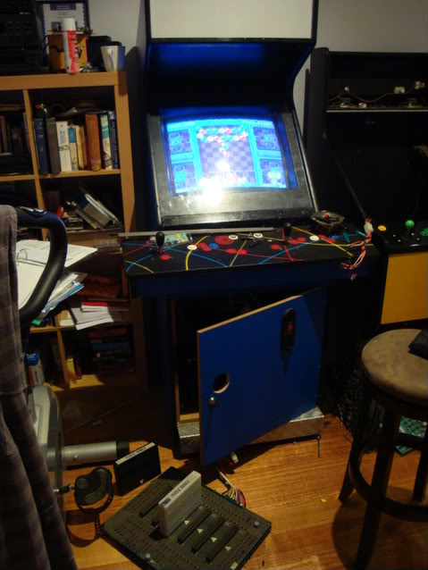
Connected it all back up, plugged it into my cab and after a bit of faff seating and reseating the carts I got it to work perfectly.
Anyone know a good method for cleaning the contacts in the cart slots? The egde of the ROM cart is easy enough, but the contacts on the slot may be a pain.
Oh and one of the two carts gives no sound, I assume it has a very dead EPROM inside, but thats for another day.
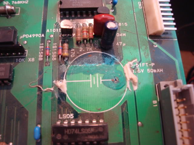
One final thing I should do to this is to rehouse the battery, its just starting to leak but has only reached the leg of a resistor at the moment, should really fit flying leads and house the battery away from the PCB, otherwise this board is living on borrowed time.
I removed the battery from the board, another 6 months to a year and it would have made a real mess, it had already eaten through the upper layer of the board down to the copper ground plane in places.
Scraped away all the crud and neutralised the alkaline muck then gave it a clean up with PCB cleaner. The board works fine without its battery, Gamedude reckons the battery is only for book-keeping functions (ie how much money has been taken, length of games, etc etc).
Gave the slots a go over with the paper trick and it seems to have worked, much more stable, originally the slightest touch on the cart would put lines through the gfx and or crash the board - crap connections clearly.
Repairer: Arcade King
Forum Thread: Neo Geo 6 Slot PCB Repair
Turned the Neo on for the first time a week ago in months only to find out one of the slots graphics were corrupted.
As I've said in the past the biggest killer of PCB's is corrosion and the Neo is one of the worst for it.
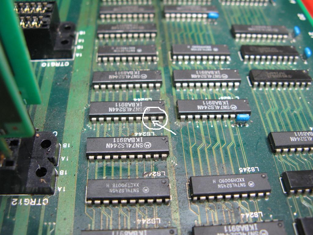
Problem: Garbled Graphics on the 6th slot. Fix: Found a dead pin on a 74LS244 @ L24. Pin 19 (active low output control) should read low (grounded) jumping pin 19 to the 244 above it solved the issue. Easy 5 minute fix.
PCB seems to have some greasy looking shit on top of it. Will grab my can of contact cleaner I got from David_AVD and give the top of the board a good clean.
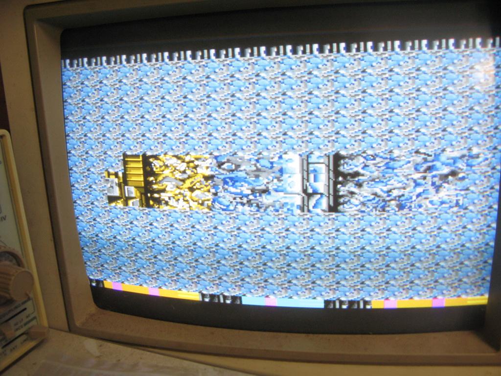
6 Slot vertical lines in graphics.
I'm documenting my findings for myself so hopefully this info will be useful to somebody else down the track.
Every neogeo cart has 2 PCB's inside it, one for Program[P1,P2 etc] and Sound Data[V1,V2 etc] the other for Graphics[C1,C2,C3 etc], Z80 Sound Program[M1] and the Text Layer[S1]. Each PCB has (or can have) 60 pins per side so that's 120 pins per PCB and 240 all up in 1 cart.
Each slot has 2 rows of pins each row is 120 pins (60 a side). Each Slot is numbered CTRG1 through to 12. So slot 1 is numbered CTRG1 (Graphics) and CTRG2 (Program) Slot 2 CTRG3 and CTRG4 etc and each side of the 120 pin rows is number A1 to A60 and B1 to B60
On a 6 slot there are "40" 74F251 8 input multiplexers(6 slot only uses 6 of the 8 inputs) so that's 204 data inputs used and 32 outputs for the GFX Data. Each cart "usually" has 2 banks of Graphic roms C1,3,5,7 and C2,4,6,8. Each 74f251 takes 1 data input from the 16 Eprom data outputs. So thats 16 x 2(Eprom Banks) = 32 27F251's. Don't worry I confuse myself sometimes.
Now I did say 40 74F251's all up, 8 located at E2,3, D1,2,3 and C1,2,3 seem to be used for the S1 Eprom which is the "Text Layer".
From my probing.
Table 1
Slot 1 uses pin 4 of the 74F251 which is input l0
Slot 2 Pin 3 l1
Slot 3 Pin 2 l2
Slot 4 Pin 1 l3
Slot 5 Pin 15 l4
Slot 6 Pin 14 l5
Pin 13 and 12 (l6,l7) are unused and conneted to +5 volts (High)
GFX roms C1,3,5,7 Data outputs to multiplexer positions. Multiplexers located below Slot 6
Table 2
D0 = K28 1A19
D1 = K29 1B19
D2 = K30 1A20
D3 = J28 1B20
D4 = J29 1A21
D5 = J30 1B21
D6 = H28 1A22
D7 = H29 1B22
D8 = H30 1A23
D9 = G28 1B23
D10 = G29 1A24
D11 = G30 1B24
D12 = F28 1A25
D13 = F29 1B25
D14 = F30 1A26
D15 = E28 1B26
GFX roms C2,4,6,7 Data outputs to multiplexer positions. D0 to D3 located below Slot 6 D4-D15 Above Slot 1
Table 3
D0 = E29 1A27
D1 = E30 1B27
D2 = D28 1A28
D3 = D29 1B28
D4 = K3 1A33
D5 = K2 1B33
D6 = J3 1A34
D7 = J2 1B34
D8 = H3 1A35
D9 = H2 1B35
D10 = G3 1A36
D11 = G2 1B36
D12 = G1 1A37
D13 = F3 1B37
D14 = F2 1A38
D15 = F1 1B38
and just for the **** of it the S1 Text Layer. S1 is usually a 27c1000 not to be confused with a 27c010 (Different pinout). Located Above slot 1
Table 4
D0 = E3 1B39
D1 = E2 1B40
D2 = D3 1B41
D3 = D2 1B42
D4 = D1 1B43
D5 = C3 1B44
D6 = C2 1A45
D7 = C1 1B46
If you can decifer my dribble above finding out the bad tracks for the vertical line problems should be easy.
So we have 3 bad slots 1,2 and 5
Lets start with slot 1 which has Vertical bars evenly spaced about 1CM apart.
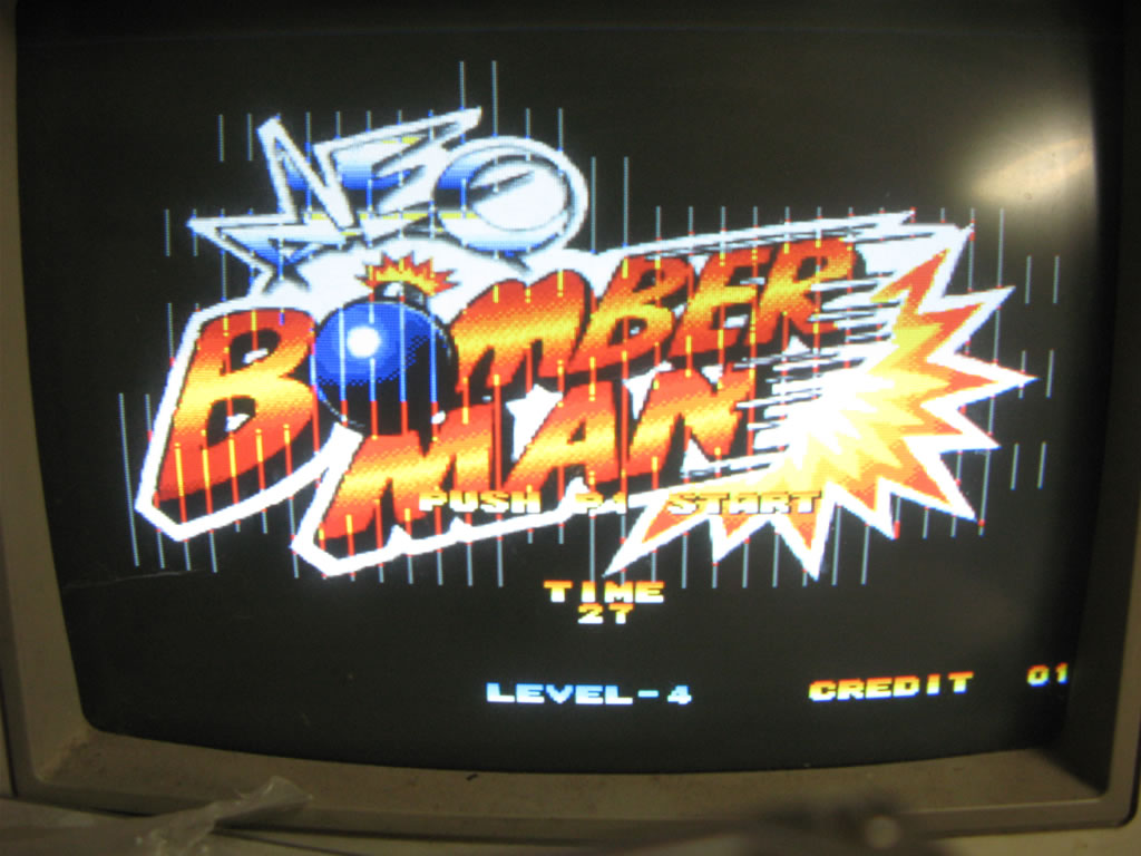
Slot 1 uses pin 4 of the 74F251's so I'll check every chip on pin 4.
Ok in less than 30 seconds found a dead pin 4 @ H3.
Now I use the Pin positions I mapped. H3 = D8 on the second bank of roms location 1A35 (Table2). You really need to know which pin strip the graphics pcb site so as a guide its ALWAYS on the arrow side. (The arrow which indicates which way the cart goes in). So the side I'm looking for is labelled CTRG1 and 1A and 1B are clearly marked on the side.
Ok time to jump a wire from pin4 on H3 to pin 1a63 on CTRG1..done and slot 1 fixed The other 2 slots Should be just as easy in fact I've got a 4 slot thats been sitting in the cupboard with the same problem that should now be easy to fix
Slot 2
This Vertical line issue looks different from the problem on Slot 1 and 5. The lines are almost every second pixel. Have a look at Pic 2, will show you what I mean.
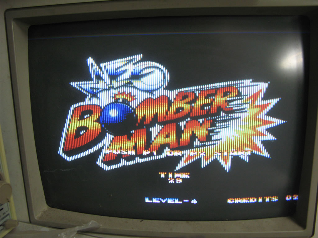
Fix: this graphic problem has to do with the S1 rom Text Layer. Using Table 1 first I check pin 3 of all the 74F251's and find C1 to be dead. using Table 4 C1 goes to pin 1B46 and the slot label is CTRG3. Run the wire and she's all fixed
Slot 5 has exactly the same symptoms as Slot 1
Slot 5 = Pin 15 on the multiplexers, found dead pin @ K3. K3= 1A33 and the slot label is CTRG9 so we run a trace from K3 pin 15 to CTRG9 pin 1A33 and FIXED!!! All slots now accounted for and working.

Its a real heartbreak to see these PCB deteriorate. Bit of a rule of thumb with graphics. Garbled graphics = Addressing problem and Lines through the graphics = Data.
I hope somebody finds this info helpful.
I spent most of the day documenting this info so please don't copy it elsewhere.