PCB Repair Logs Bubble Bobble
Bubble Bobble
 |
|
| Manufacturer | Taito |
|---|---|
| Year | 1986 |
| PCB Image | Bubble Bobble PCB |
| Pin Out | Reserved |
Repairer: Womble
Forum Thread: Bubble Bobble PCB Repair
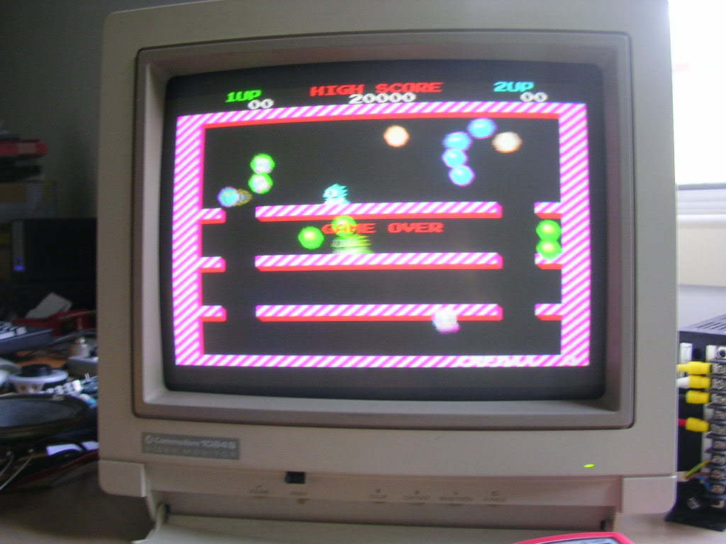
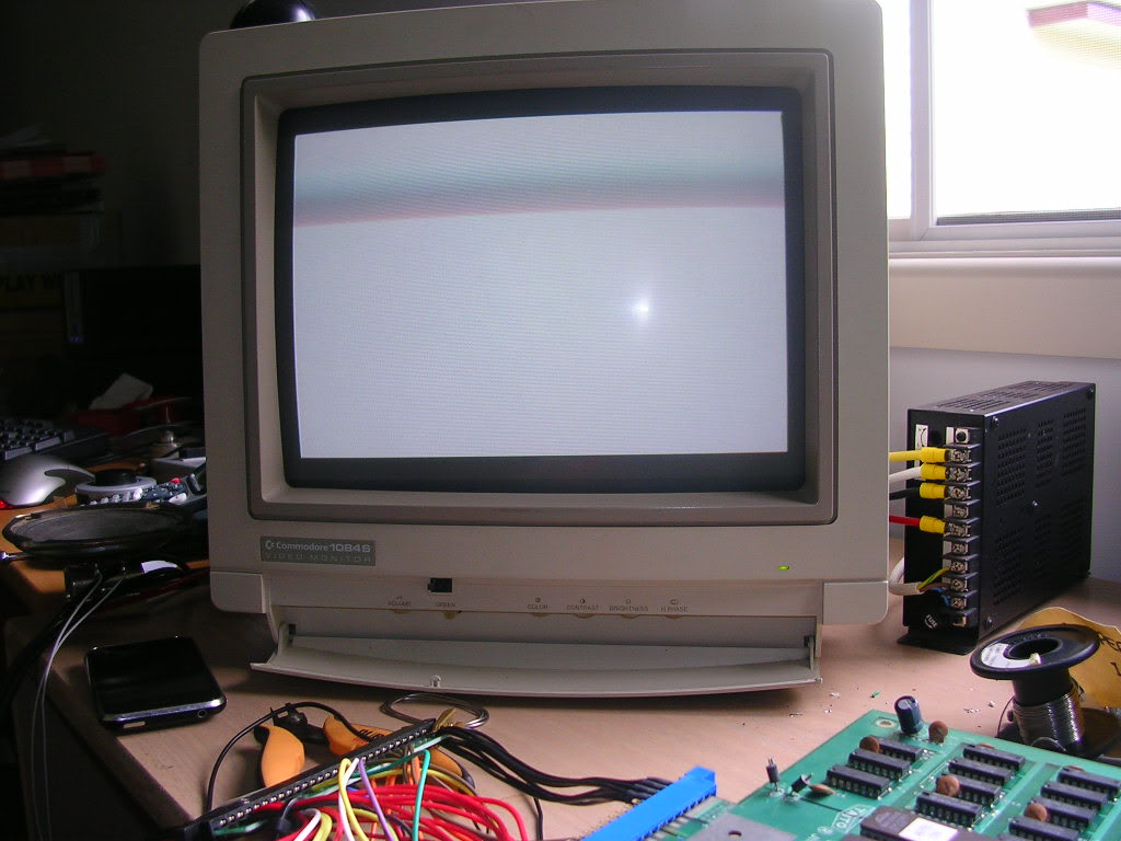
I have had Stu's original Taito Bubble Bobble PCB in my toy room for ages and finally got an afternoon to myself to take a look at it. The fault was that it would run blind, giving only a white screen. Firing this up on the repair bench with the harness from my board gave this, sound effects but not much else.
This game is a dual pcb set, comprising a video board and cpu board, the fact the game ran without graphics meant the fault was likely to be on the video board. For video faults the issue will usually be on the video board but with games that do not run at all you can't assume the fault will be on the CPU board , there is plenty of opportunity to crash the game on the video board alone. Anyway in this case as I had a board set handy I just swapped my video board onto Stu's CPU board and the game fired up with graphics, so I knew the fault was isolated to the video board.
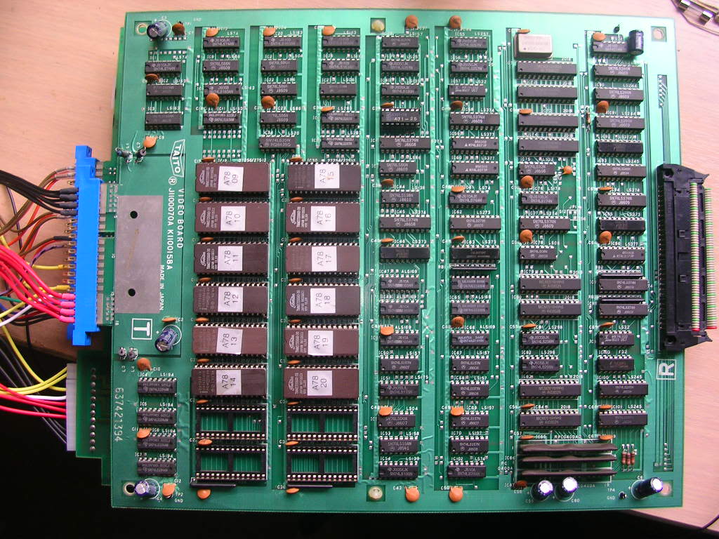
The most likely candidate was bad RAM so I hit the 2018 SRAMs with the scope looking to see if the video processing was actually running. Only a four of the eight 2018 chips had any activity on them, the others were totally silent, on both buses. The data output on the active chips (IC71,72,73, and 74) looked fairly messed up, there were no clean transitions between logic high and low, the trace on the scoped showed a stepped output which is indicative of more than one chip trying to drive the bus lines at once. The schematics proved very helpful showing how things were laid out, the 4 chips were acting as two pairs, each pair had control of half the 16bit data bus.
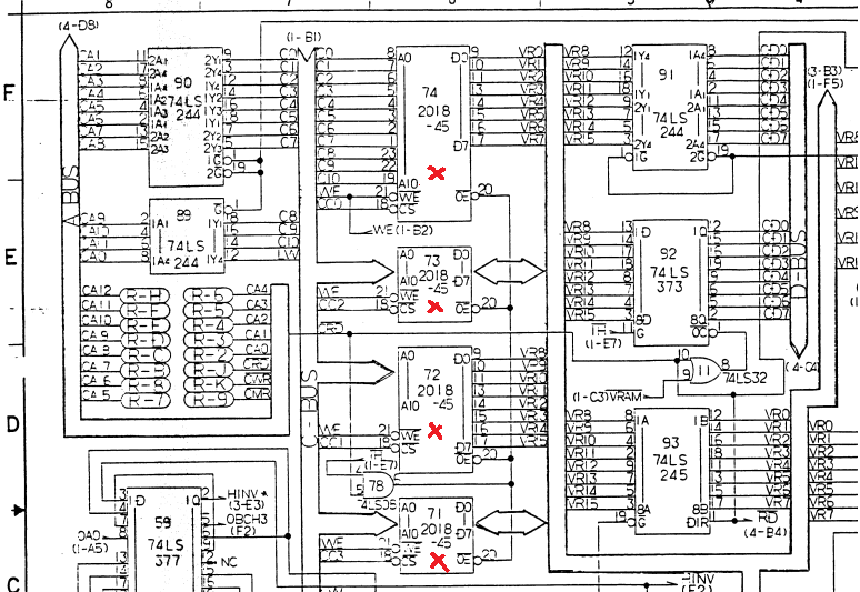
When RAM chips are paired there needs to be a mechanism to ensure that only one of the pair can drive the data lines at a time, otherwise their outputs fight each other and the data is totally corrupted. There are two ways to silence a 2018 chip, one is to use the /OE (output enable) pin, when this is logic high the outputs of the chip are isolated from the bus. The other method is to deselect the chip entirely with the chip select pin /CS. This is a slower method then using /OE but puts the chip in a low power mode, often this is simply tied to ground and the control uses the /OE pins alone. On this board both /OE and and /CS are employed and on each of the pairs only one of the /CS pins had any activity, the other was held low which means those chips would always be fighting their partner chips to drive the data lines. The /OE lines are common and therefore cannot be used to control these chips individually on this board, so there was a fault upstream of 2 out of the 4 /OE pins, which according to the schematics are lines called C00, C02, C01 and C03 on the "C-BUS".
These lines are the four outputs of an LS157 at IC38, its inputs looked healthy on the scope so I slapped a spare LS157 in my HP logic comparator and clipped the probe on to the one on the board. It reported that the chip was fine; all it does is take the input signals that the on-board chip is getting and feeds them into the test chip, it then compares the outputs of bothe chips and if there is any difference it lights up a LED corresponding to the mismatching output pin. In this case the only LED lit was the power LED so the known good chip was doing the exact same thing as the one on the board. What it did inadvertently prove was that I was at least on the right track, as I connected the clip the screen flipped to this...
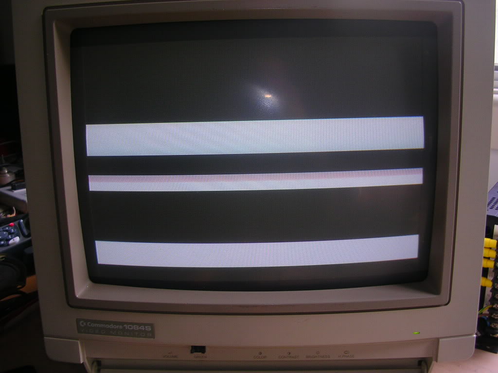
...the bars were moving and this was the background of the high score table being drawn, when the clip was fully seated the effect was lost. LS157s are multiplexer chips that take 4 pairs of signals and generate 4 single signals, so it was likely that two of the pairs had input signals that were incorrect. One set of 4 signals came from an LS139 address decoder chip and its output signals were all active and looked healthy. The other set of 4 signals were silent, two high and two low. All four are derived from the same signal split in two, and one half fed through an inverter gate on the LS4 at IC21, and the inverted and non inverted outputs split again giving two of each. I had no way to know if this steady state was correct or not on this board so I swapped my board onto the bench and hit the input to the LS04 with the scope - activity, lots of it, that line should not be silent!
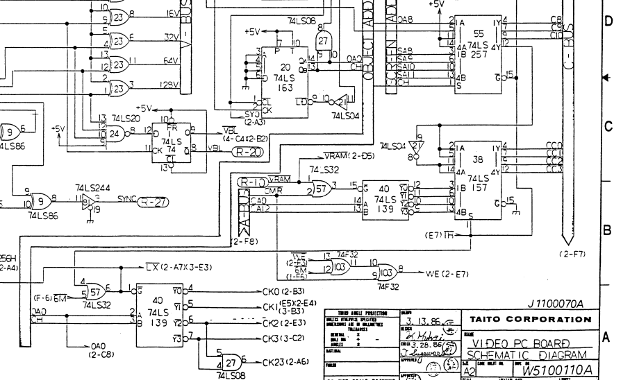
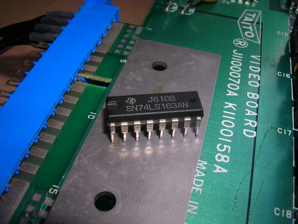
The feeder line for all this silence was the 4Y output on the 74LS257 at IC55, another multiplexer fed by the screen address bus and the object address bus according to the schematics. So I dropped an LS257 into my comparator and connected it to IC55, the results were strange, of the 4 outputs (1Y-4Y) the only one that was shown as ok was 4Y, the one I suspected. The other three were flagged as bad, in fact this test failed all the LS257s on the board, and the ones on my board which had to be fine. The LS257s on board are from Texas Instruments and I have heard that these have slightly different timings than non Ti ICs, in fact I read somewhere that on Galaga boards only Ti chips should be used due to this, may or may not be true, but it would explain why the comparison to a non-Ti chip gave errors. Anyway, the fact that line 4Y was marked as good was the clue, it was correct because it was never changing, the erroneously faults were timing related, as it never changed there were no events to be mis-timed. To simply rule out the chip itself I de-soldered it and tested it on my EPROM reader, it passed the test fine, which left the control lines as the only thing that could be suspect. The line on an LS257 that can affect whether a single output of the four are selected or not is the select line "S", and this was fed by the "Qb" output on the 74LS163 at IC20...
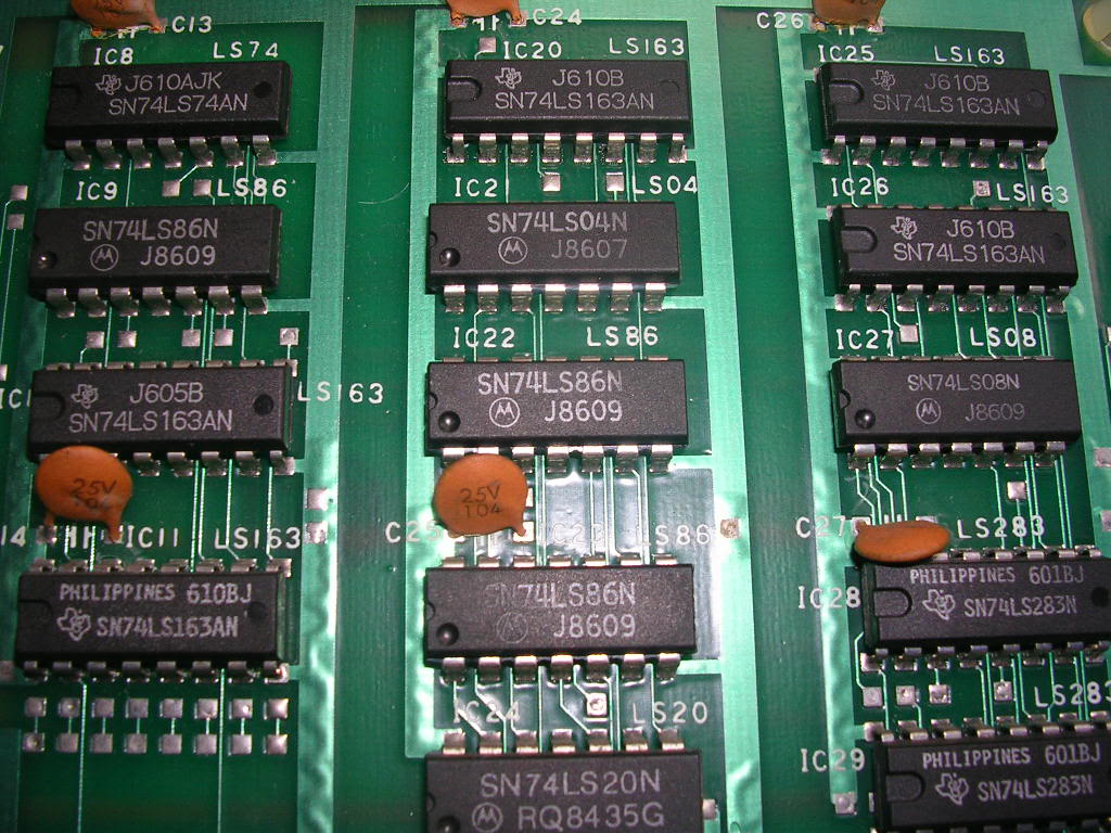
...the outputs were active on the scope but looked faint and somewhat unstable. These are not common chips and had to go through my entire scrap pile until I reached the a board at the very bottom that had one I could scavenge. A quick de-solder and test on the ERPOM reader to confirm it was ok and it ended up in the logic comparator as the known good chip. When the board was powered up with the clip attached to IC20 I got this...
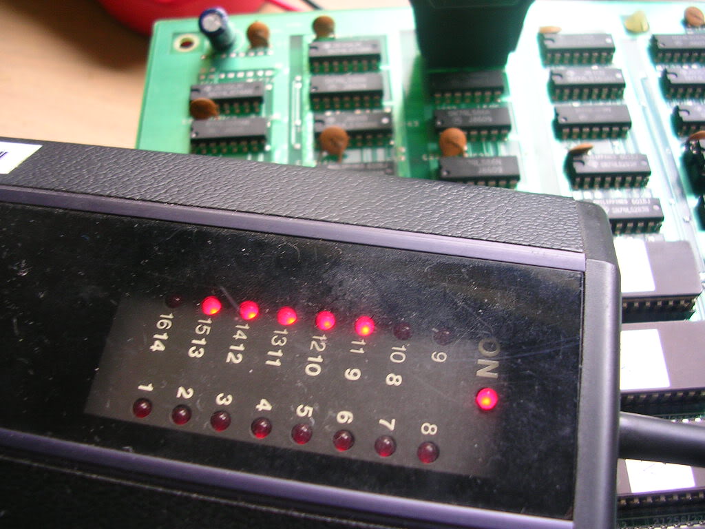
... all outputs bad! Just to rule out the timing issue again I tested the other LS163s on the board and they all passed. So I de-soldered the original...
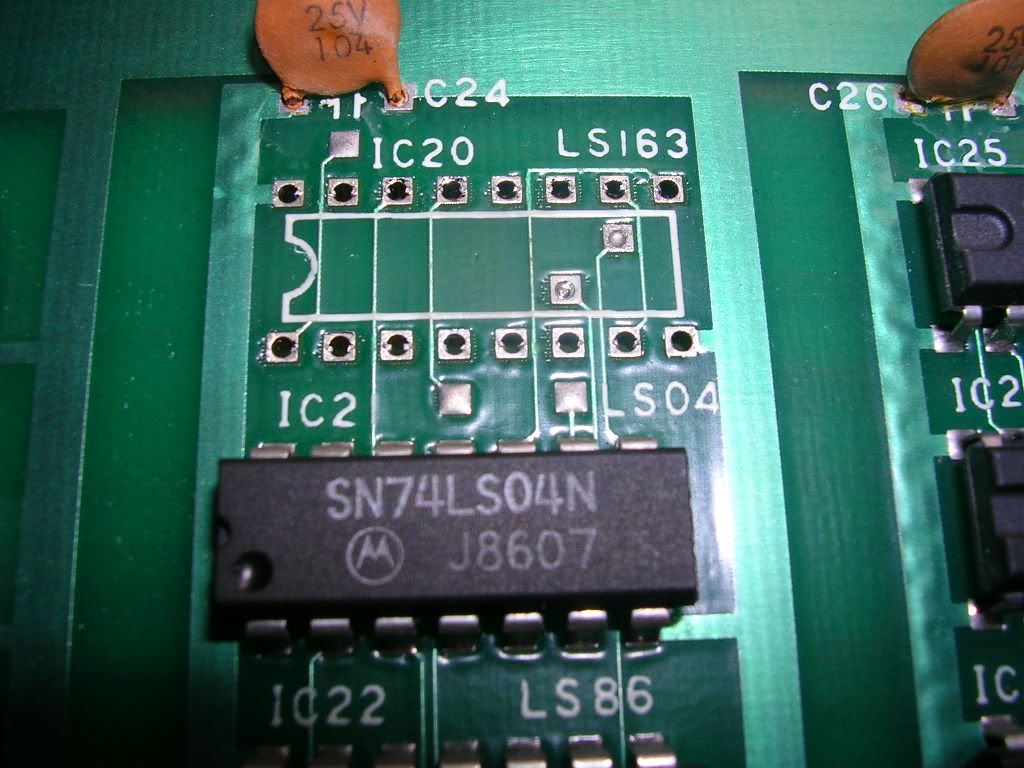
...and tested it off board to confirm the outputs were not jammed by the board and that the chip was indeed faulty...
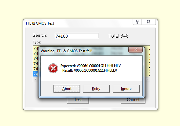
...which it was!
So the recently de-soldered 74LS163 was soldered in its place, the board connected back up and the power flipped on...

...fixed!
Have noticed that faults often seem to occur right on the edges of boards, right where static'y fingers can get to, or perhaps where things are prone to being shorted out against something when powered up.
Great to save a classic!
